Liquid crystal display device and method for driving the same

Inactive Publication Date: 2002-09-12
PANASONIC CORP
View PDF0 Cites 12 Cited by
  • Summary
  • Abstract
  • Description
  • Claims
  • Application Information

AI Technical Summary

Benefits of technology

0020] The object of the present invention is to solve the above-mentioned problems thereby to provid

Problems solved by technology

Further, power-consumption of these operational amplifiers is a serious pro

Method used


Image

  • Liquid crystal display device and method for driving the same
  • Liquid crystal display device and method for driving the same
  • Liquid crystal display device and method for driving the same

Examples


Embodiment Construction

[0054] Hereafter, preferred embodiments of the present invention will be described in detail referred to as the attached drawings.

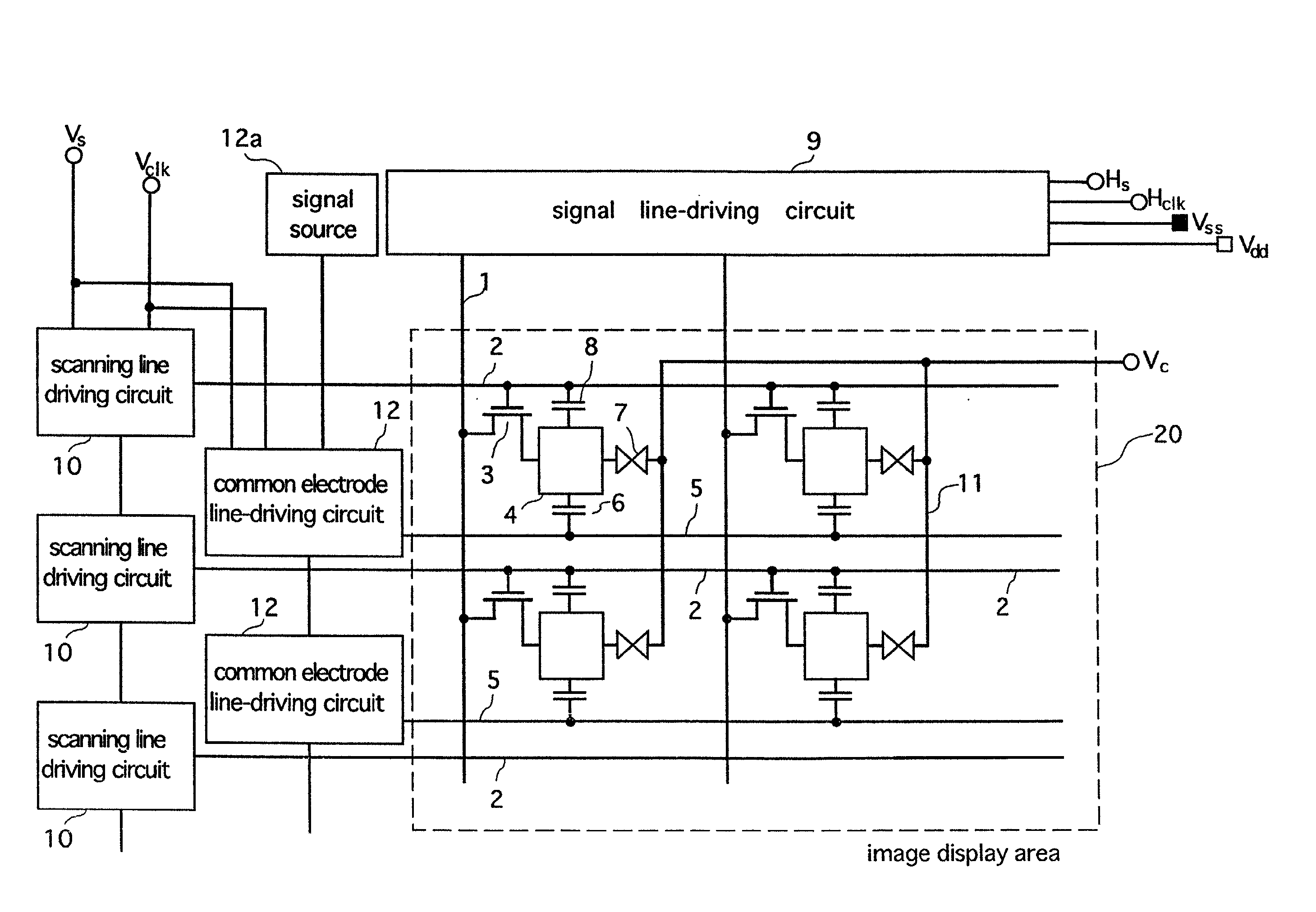
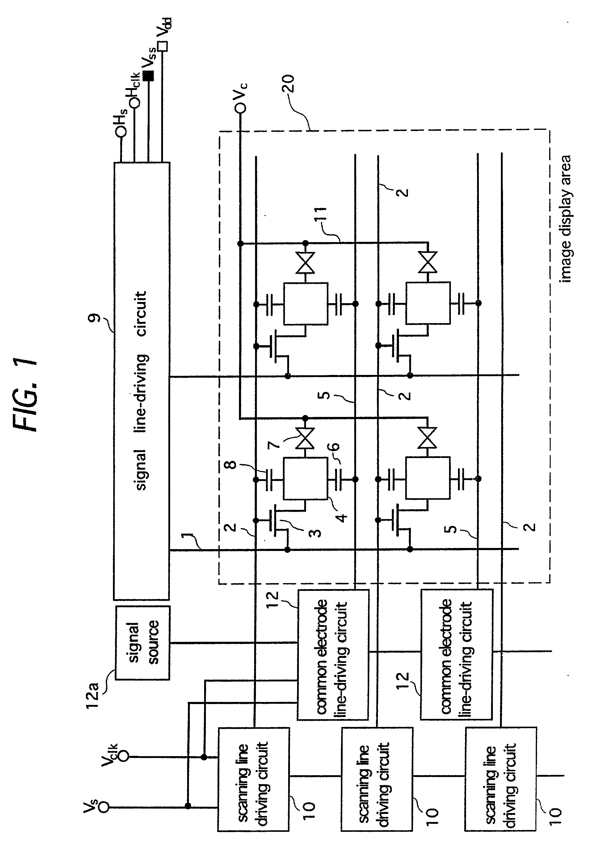
[0055] A schematic structure of a liquid crystal display device in this embodiment is shown in FIG. 1.

[0056] In an image display area 20, signal lines 1 and scanning lines 2 are provided so as to cross at right angles with each other. A switching element 3 is provided around each intersection point of the signal line 1 and scanning line 2. The switching element 3 is for controlling a connection between the signal line 1 and a pixel electrode 4, based on a scanning signal inputted from a scanning signal-driving circuit 10 via the scanning line 2. A liquid crystal layer 7 is driven by an electric field formed between the pixel electrode 4 and a counter electrode 11.

[0057] Plural common electrodes 5, each making a pair with the scanning line 2, are provided in substantially parallel therewith. Between the pixel electrode 4 and the common electrode line 5, th...


PUM


Abstract

According to the present invention, common electrode lines each making a pair with scanning line are provided and a potential of the common electrode line is alternately changed between two predetermined values to make amplitude in potential of pixel electrode larger than that of image signals thereby decreasing the amplitude of image signals. The present invention also realizes a signal source low in price and further in power-consumption therefor, thereby realizing small-sized and low-priced liquid crystal display devices suitable for portable apparatus.

Description

BACKGROUND OF THE INVENTION[0001] The present invention relates to an active matrix liquid crystal display device, especially to an improvement thereof for decreasing amplitude of image signals from a signal-side circuit and those of scanning signals from a scanning-side circuit while increasing utility of the device.[0002] For active matrix liquid crystal display devices, there is proposed an opposite constant charge coupling driving in which a storage capacitance is provided between a preceding scanning line and a pixel electrode for applying a bias-voltage to a liquid crystal in, for example, "Flat Panel Display '93 (published by Nikkei Business Publications Inc.)" on pp. 128-131. The proposal is for suppressing maximum amplitude of image signals to 5 V or around, and further for suppressing an influence caused by a parasitic capacitance or an internal DC voltage application.[0003] The above-mentioned system accompanies with an increase in amplitude of scanning signals, on the ot...

Claims


Application Information

Patent Timeline
IPC IPC(8): G09G3/36
CPCG09G3/3655G09G2300/0876G09G2320/0219G09G2320/0247G09G2320/0606G09G2320/0626
Inventor ADACHI, KATSUMIYAMAKURA, MAKOTO
Owner PANASONIC CORP
Why Eureka
Try Eureka