Semiconductor unit, and power conversion system and on-vehicle electrical system using the same

a technology of semiconductor devices and power conversion systems, which is applied in the direction of semiconductor devices, heat exchange apparatus, and semiconductor/solid-state device details, etc., can solve the problems of not revealing the thermal connection and electrical insulation between the semiconductor devices and the radiator mechanism, and the thickness of the solder or brazing material used in mounting the second and third radiators to the upper surface of the semiconductor devices is not uniform, so as to improve the electrical insulation and reduce the thermal resistance. , the effect of high reliability

Inactive Publication Date: 2007-05-03
HITACHI LTD
View PDF4 Cites 129 Cited by
  • Summary
  • Abstract
  • Description
  • Claims
  • Application Information

AI Technical Summary

Benefits of technology

[0018] With this arrangement, a more compact, lower-cost, and higher-reliability power conversion system and on-vehicle electrical system can be achieved.
[0019] This invention improves the electrical insulation between the semiconductor device and the radiator mechanism and r

Problems solved by technology

The recent challenge of electrical systems equipped with an electrical circuit module having semiconductor devices is to achieve more compact, lower-cost, and higher-reliability systems.
For example, the important challenge of cars is to achieve more compact, lower-cost, and higher-reliability electrical systems equipped with an electrical circuit module having semiconductor devices.
In this respect, the device described in JP-A-2004-296663 disclosed the structure

Method used


Image

  • Semiconductor unit, and power conversion system and on-vehicle electrical system using the same
  • Semiconductor unit, and power conversion system and on-vehicle electrical system using the same
  • Semiconductor unit, and power conversion system and on-vehicle electrical system using the same

Examples


first embodiment

[0059] FIGS. 1 to 13 show the structures of a semiconductor unit according to the invention, an on-vehicle inverter using the semiconductor unit, and a hybrid electric vehicle using the on-vehicle inverter.

[0060] Referring to FIGS. 1 to 5, the structure of the semiconductor unit of this embodiment will be described.

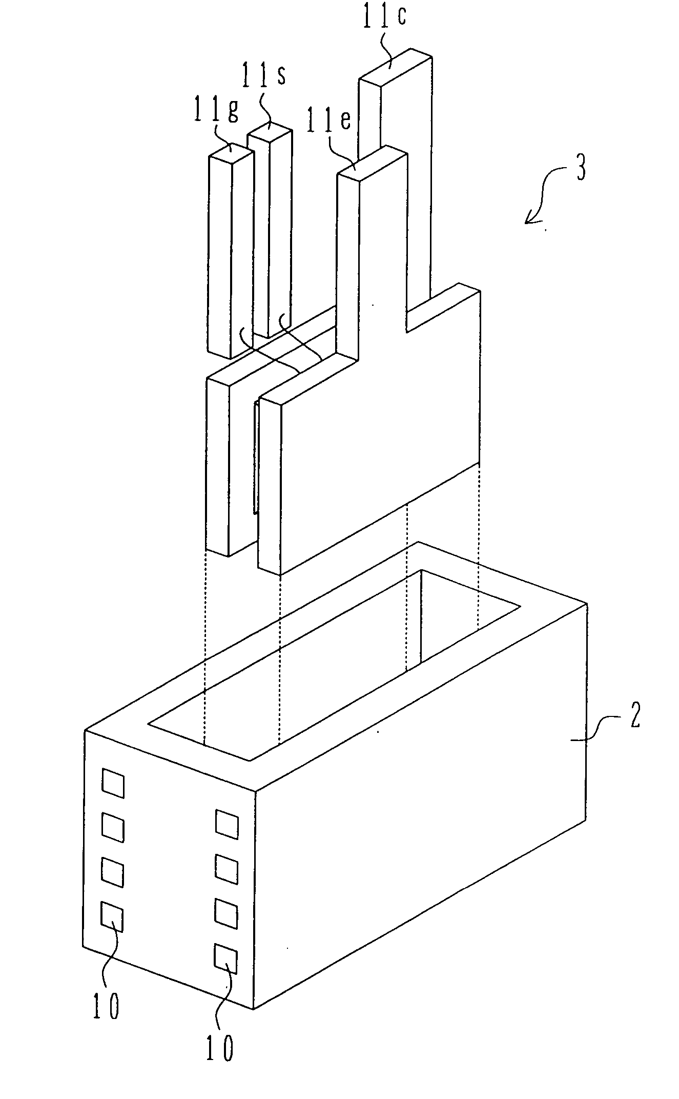
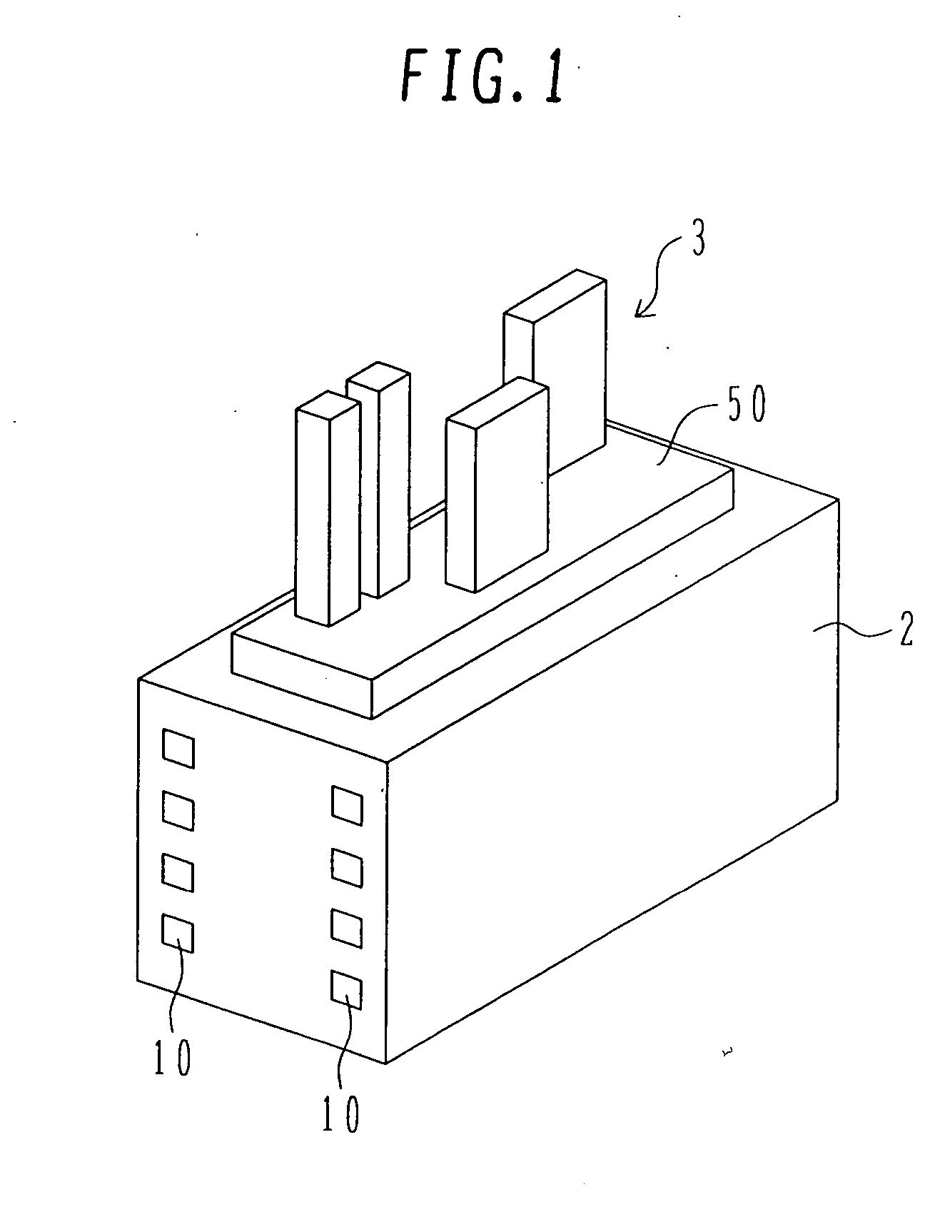
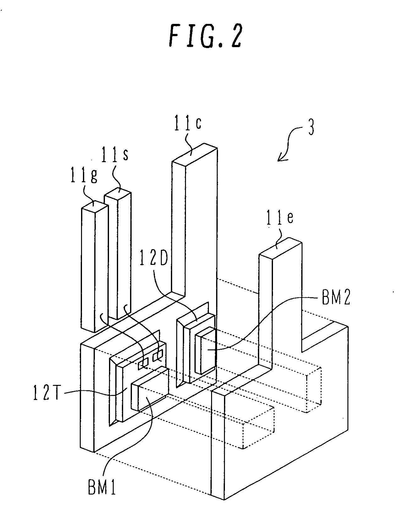
[0061]FIG. 1 is a perspective view of the semiconductor unit according to the first embodiment of the invention; FIG. 2 is a perspective view of a semiconductor device used in the semiconductor unit according to the first embodiment; FIG. 3 is an exploded perspective view of the semiconductor unit according to the first embodiment; FIG. 4 is a side sectional view of the semiconductor unit according to the first embodiment; and FIG. 5 is a front view of the semiconductor unit according to the first embodiment. In FIGS. 1 to 5, like elements are given like reference numerals.

[0062] Referring first to FIG. 1, the semiconductor unit of the embodiment is made up of a semicon...

second embodiment

[0169] Referring to FIGS. 14 and 15, the structure of a semiconductor unit according to the invention will be described.

[0170]FIG. 14 is a perspective view of the semiconductor unit according to the second embodiment of the invention; and FIG. 15 is a sectional view of the semiconductor unit of the second embodiment. The same numerals as in FIGS. 1 to 5 indicate the same components.

[0171] In this embodiment, as shown in FIG. 14, a power semiconductor device 3A has a plurality of insulative high-thermal-conductivity projections 54 on the surface of the emitter lead 11e (on the surface facing the inside of the radiator base 2). Likewise, the insulative high-thermal-conductivity projections 54 (not shown in FIG. 14) are provided also on the surface of the collector lead 11c (on the surface facing the inside of the radiator base 2).

[0172] The insulative high-thermal-conductivity projections 54 are made of a material of electrical insulation and high thermal conductivity. One example i...

third embodiment

[0178] Referring next to FIGS. 16 and 17, a semiconductor unit according to the invention will be described.

[0179]FIG. 16 is a front view of the semiconductor unit according to the third embodiment of the invention; and FIG. 17 is a sectional view of the semiconductor unit of the third embodiment taken along line B-B of FIG. 16. The same numerals as in FIGS. 1 to 5 indicate the same components.

[0180] The embodiment has electrically insulative support jigs 56A and 56B in the radiator base 2 as shown in FIGS. 16 and 17, with which the power semiconductor device 3 is retained, and molded with the high-thermal-conductivity resin 50. The structure of the power semiconductor device 3 is the same as that shown in FIG. 2.

[0181] As shown in FIG. 17, in the state in which the power semiconductor device 3 is insert-molded in the hollow radiator base 2 with the high-thermal-conductivity resin 50, the high-thermal-conductivity resin 50 is present between the collector lead 11c and the sensor l...


PUM


Abstract

A semiconductor device includes a semiconductor chip and leads electrically connected to the electrodes of the semiconductor chip. A hollow radiator base houses the semiconductor device which is molded with high-thermal-conductivity resin having an electrical insulating property. The radiator base has a cooling-medium channel therein or radiating fins on the outside. Alternatively, the radiator base is housed in a second radiator base.

Description

BACKGROUND OF THE INVENTION [0001] 1. Field of the Invention [0002] The present invention relates to a semiconductor unit, and a power conversion system and an on-vehicle electrical system using the same. [0003] 2. Description of the Related Art [0004] For semiconductor devices, particularly, for power semiconductor devices that switch large currents, double-side cooling semiconductor unites that cool the power semiconductor devices from both sides are being contemplated because of the high heating values. The performance needed to cool semiconductor devices depends on the environments of electrical systems to which an electric circuit module equipped with the semiconductor devices is to be mounted. For example, power conversion systems for vehicles require high performance to cool the electrical systems because of the on-vehicle environment and operating environment. [0005] An example of conventional double-side cooling semiconductor units is disclosed in JP-A-2004-296663, which is...

Claims


Application Information

Patent Timeline
IPC IPC(8): H01L23/02B60L50/16
CPCF28F3/12H01L2924/30107H01L23/473H01L25/071H01L25/072H01L2924/13091H01L24/33H01L2924/13055H01L23/3675H01L2924/3025H01L2224/32245H01L2224/33181H01L2224/48247H01L2224/73215H01L2224/73265H01L2924/1305H01L2924/1306H01L2924/00H01L2924/00012H01L2924/351H01L2924/181H01L2224/48091H01L24/73H01L2224/291H01L2924/14H01L2224/33H01L2924/00014H01L2924/014
Inventor NAKATSU, KINYAMIYAZAKI, HIDEKITAKEZAWA, YOSHITAKAISHII, TOSHIAKIHOZOJI, HIROSHI
Owner HITACHI LTD
Why Eureka
Try Eureka