
Method for producing silicon single crystal

a single crystal and silicon technology, applied in the direction of crystal growth process, crystal growth process, polycrystalline material growth, etc., can solve the problem of significant decrease in the yield of the crystal, and achieve the effect of preventing the dislocation of the single crystal, accelerating the flow rate of argon gas flowing, and efficient discharg

Inactive Publication Date: 2002-09-19
SUMITOMO MITSUBISHI SILICON CORP
View PDF0 Cites 7 Cited by
  • Summary
  • Abstract
  • Description
  • Claims
  • Application Information

AI Technical Summary

Benefits of technology

[0012] However, if a silicon single crystal is again produced by dissolving the single crystal with dislocations when this MCZ method is applied to the production of a silicon single crystal having a diameter as large as 200 mm or more by using a large diameter crucible having a diameter of 500 mm or more, this poses the problem that a dislocation of the single crystal occurs frequently in the step of forming the shoulder portion of the single crystal, which significantly decreases the yield of the crystal.
[0013] This invention has been made in view of the above situation and it is an object of the present invention to provide a method for producing a silicon single crystal, the method capable of suppressing the dislocation of a single crystal and improving the yield of the silicon single crystal in a MCZ method even if the single crystal with dislocations is dissolved to produce the silicon single crystal again.
[0018] Because the temperature of the melt must be raised to dissolve the single crystal with dislocations in general, the evaporation of SiO from the surface of the melt and the dissolution of the inside wall of the quartz crucible which is in contact with the melt are promoted. For this reason, it is considered that in the case of dissolving the single crystal with dislocations in such a condition that a magnetic field is applied to the melt, foreign substances contained in the melt exist as it is in the vicinity of the surface of the melt for a long time, so that they are carried on the flow running towards the center of the crucible from the wall of the crucible and easily reach the growth boundary of the single crystal, causing frequent dislocations.
[0020] Specifically, if the single crystal with dislocations is dissolved in such a condition that no magnetic field is applied to the melt in the crucible, the condition of the melt which rejects the access of foreign substances on the surface of the melt to the center of the crucible is created. The dislocation of the single crystal can be prevented by pulling the silicon single crystal under the application of a magnetic field in this condition of the melt.
[0021] Also, when the single crystal with dislocations is dissolved, it is desirable that the flow rate of argon gas to be supplied to the single crystal producing apparatus be designed to be 100 L / min or more and the pressure in the apparatus be designed to be 6700 pa or less. This accelerates the flow rate of argon gas flowing over the surface of the melt, so that SiO evaporated from the surface of the melt can be efficiently discharged to the outside of the apparatus efficiently and foreign substances floating on the surface of the melt can be driven towards the wall of the crucible.

Problems solved by technology

However, if a silicon single crystal is again produced by dissolving the single crystal with dislocations when this MCZ method is applied to the production of a silicon single crystal having a diameter as large as 200 mm or more by using a large diameter crucible having a diameter of 500 mm or more, this poses the problem that a dislocation of the single crystal occurs frequently in the step of forming the shoulder portion of the single crystal, which significantly decreases the yield of the crystal.

Method used


Image

  • Method for producing silicon single crystal
  • Method for producing silicon single crystal
  • Method for producing silicon single crystal

Examples


Embodiment Construction

[0028] An embodiment of the present invention will be hereinafter explained with reference to the drawings.

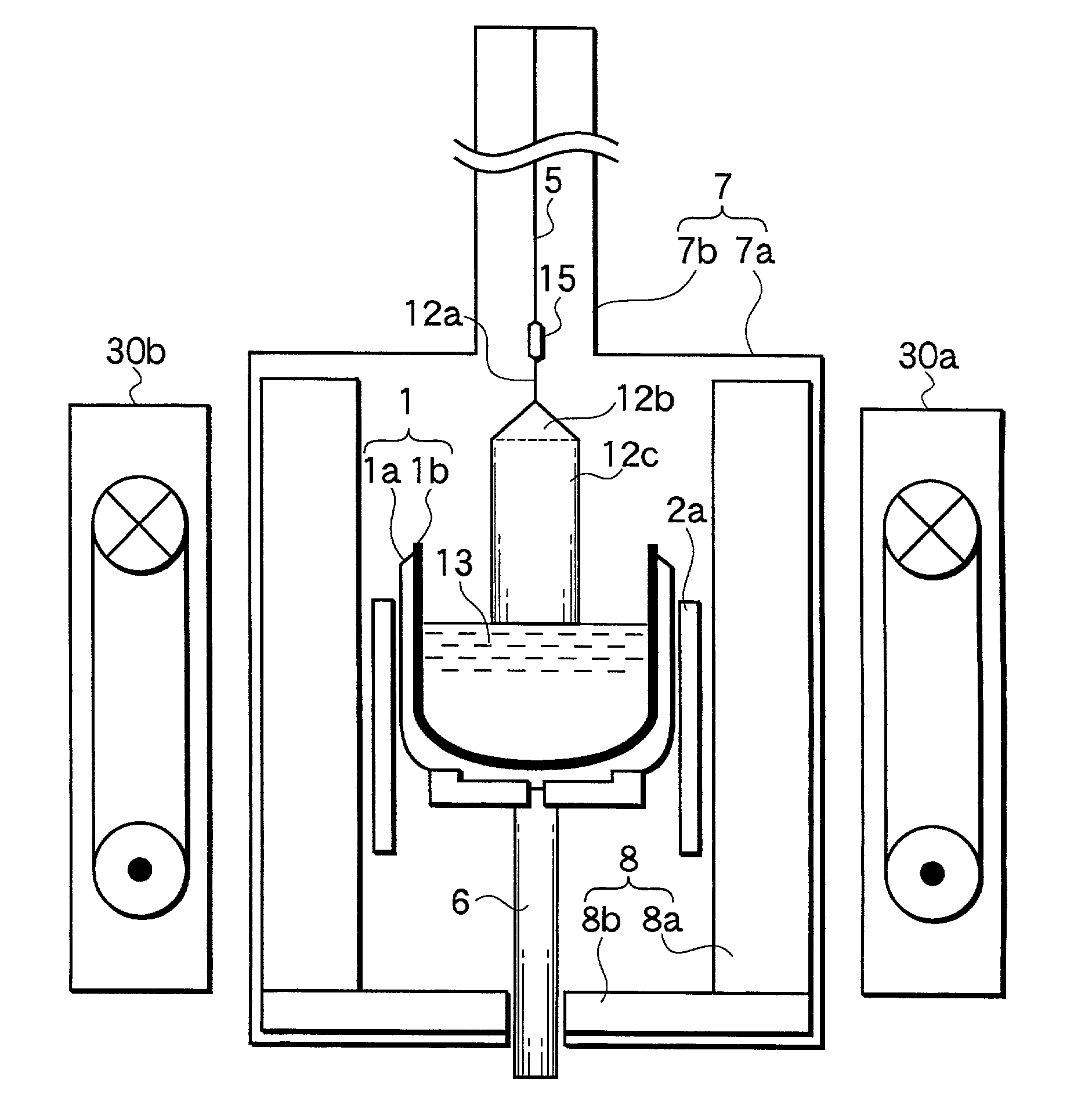
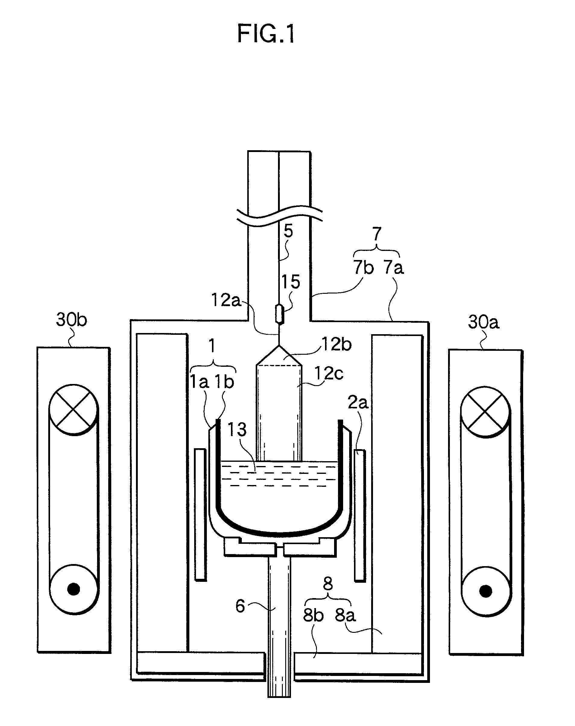
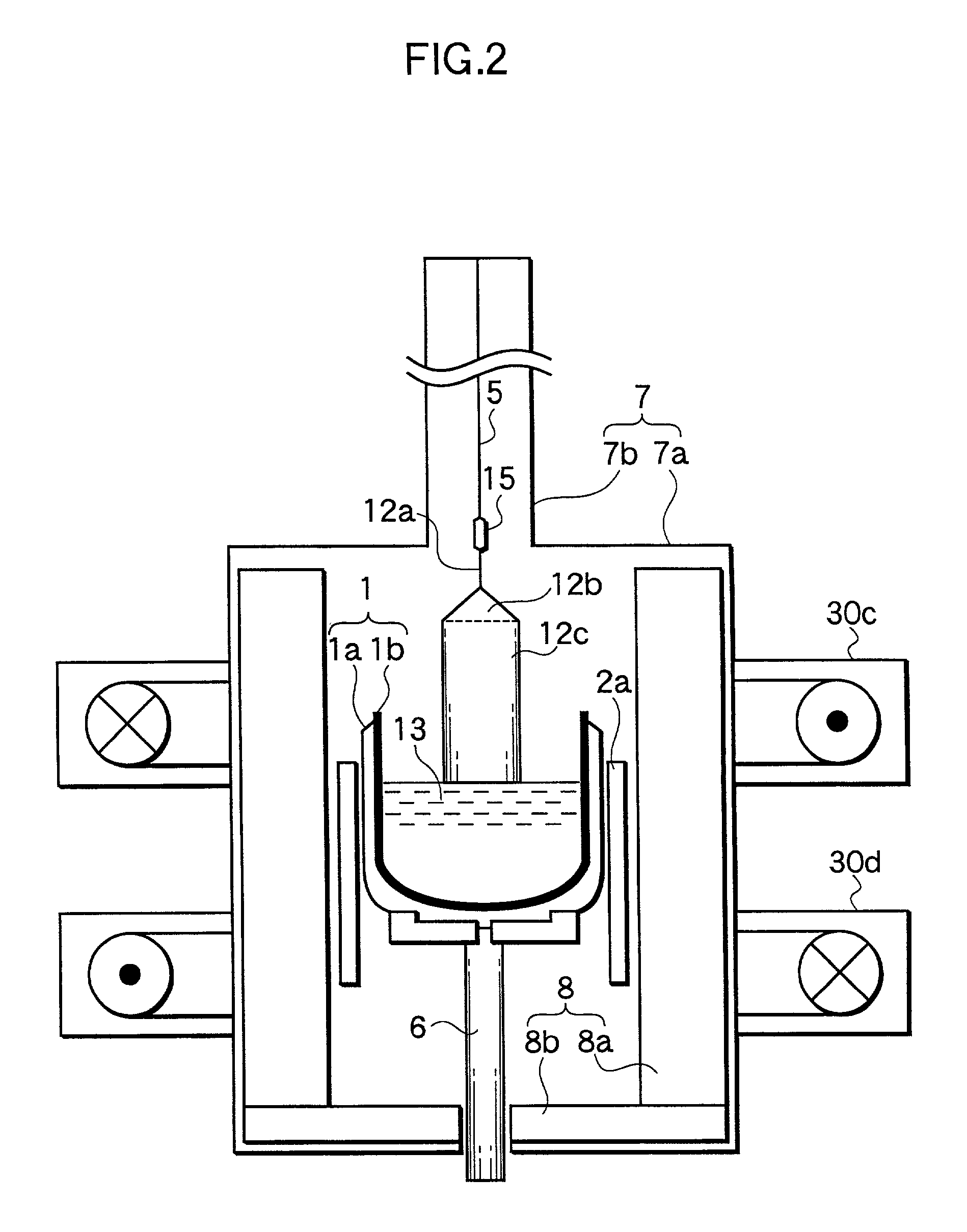
[0029] FIG. 1 is a schematic sectional view of an apparatus for producing a single crystal, the apparatus being used to practice a method for producing a silicon single crystal according to the present invention. In the figure, the reference numeral 7 represents a cylindrical chamber. The chamber 7 is constituted of a main chamber 7a having a cylindrical form and a cylindrical pull-chamber 7b secured directly to the main chamber 7a. A heater 2 is arranged on the outside of the crucible 1, a heat insulating cylinder 8a is arranged concentrically on the outside of the heater 2 and a heat insulating board 8b is arranged on the bottom of the main chamber 7a.

[0030] A raw material is filled in the crucible 1 and melted by the heater 2. A pulling shaft 5 which can be rotated on the same axis as a support shaft 6 and is movable vertically is formed such that it is hung through the pull...


PUM


Abstract

A method for producing a silicon single crystal, the method being capable of suppressing the dislocation of a single crystal. When a silicon single crystal is produced by a Czochralski method in which a horizontal magnetic field or a cusp magnetic field is applied and the single crystal during growth is dislocated, the single crystal with dislocations is dissolved in a nonmagnetic field condition and thereafter a magnetic field is applied again to pull up the silicon single crystal. The flow rate of argon gas is designed to be 100 L / min or more and the pressure in a furnace is designed to be 6700 pa or less when the single crystal with dislocations is dissolved.

Description

BACKGROUND OF THE INVENTION[0001] 1. Field of the Invention[0002] The present invention relates to a method for producing a silicon single crystal, and more particularly, to a method for producing a silicon single crystal, the method capable of suppressing a dislocation of a silicon single crystal.[0003] 2. Description of the Related Art[0004] There are many methods for producing a silicon single crystal. A typical one among these methods is a Czochralski method (CZ method). FIG. 3 is a typical sectional view showing a single crystal producing apparatus used in the CZ method. In the figure, the reference numeral 1 represents a crucible disposed in a chamber. The crucible 1 is constituted of an internal layer support container 1a made of quartz and having a bottomed cylindrical form and an external support container 1b made of graphite and having the same bottomed cylindrical form, the external support container being fitted so as to support the outside of the internal layer support ...

Claims


Application Information

Patent Timeline
IPC IPC(8): C30B29/06C30B15/00C30B15/30
CPCC30B15/305C30B29/06
Inventor FUJIWARA, HIDEKINISHIMOTO, MANABUMIYAMOTO, ISAMUMORITA, HIROSHI
Owner SUMITOMO MITSUBISHI SILICON CORP
Learn More