Board-level EMI shield that adheres to and conforms with printed circuit board component and board surfaces

a printed circuit board and shielding technology, applied in the field of emi protective measures for printed circuit boards, can solve the problems of lack of shielding effectiveness provided by conventional metallic boxes, use of such metallic boxes, and emi, and achieve the elimination of size restrictions on the cooling holes and fan grilles on the product enclosures, the effect of reducing the cost and weight of sheet metal and eliminating the constraints on package design

Inactive Publication Date: 2002-09-19
HEWLETT PACKARD DEV CO LP
View PDF22 Cites 68 Cited by
  • Summary
  • Abstract
  • Description
  • Claims
  • Application Information

AI Technical Summary

Benefits of technology

0013] Another advantage of the present invention is that it does not create a thermal insulation of "dead air" space around the shielded components. In fact, because the conformal EMI shield is a thin, continuous layer that is physically attached to the printed circuit board, it actually promotes the distribution of heat away from the coated printed circuit board regions rather than serving as a thermal insulator. Specifically, the conformal EMI shield conducts heat away from the component to the surface of the conductive coating where it is either dissipated through convection to the surrounding environment or conducted to a heat sink.
0014] As noted, conventional product enclosures include cooling holes and fans to circulate air around the printed circuit board and metallic EMI boxes. An associated benefit of the present invention is that the size restrictions on the cooling holes and fan grills on the product enclosures is eliminated since there is no longer a need to remove heat from a high temperature metallic EMI box on the printed circuit board.
0015] A further advantage of the present invention is that it eliminates the need for all other types of EMI shielding components. In particular, by eliminating the conventional metallic EMI boxes reduces the cost and the weight of the sheet metal. This, in turn, eliminates the constraints on package design imposed by such conventional approaches. Furthermore, the associated shielding components such as gaskets and spring contacts are eliminated.
0016] A number of aspects of the invention are summarized below, along with different embodiments that may be implemented for each of the summarized aspects. It should be understood that the embodiments are not necessarily inclusive or exclusive of each other and may be combined in any manner that is non-conflicting and otherwise possible. It should also be understood that these summarized aspects of the invention are exemplary only and are considered to be non-limiting. Also, various aspects of the present invention and embodiments thereof provide certain advantages and overcome certain drawbacks of conventional techniques. Not all aspects and embodiments share the same advantages and those that do may not share them under all circumstances. These disclosed aspects, some of which are summarized below, are not to be construed as limiting in any regard; they are provided by way of example only and in no way restrict the scope of the invention.
0017] In one aspect of the invention, an electrically continuous conformal EMI protective shield for coating a region of a printed circuit board is disclosed. The conformal EMI shield includes a low viscosity, high adherence dielectric coating configured to be applied directly to surfaces of one or more regions of the printed circuit board. The dielectric coating configured to provide a layer of insulation that adheringly coats all surfaces of the printed circuit board region. A low viscosity conductive coating configured to be applied at least to the dielectric coating to prevent electromagnetic emissions generated by the printed circuit board from emanating beyond the conformal coating. The EMI shield adheres directly to and conforms with the surface of the printed circuit board region.
0018] The dielectric coating has a combination of adhesion and viscosity that, when applied, enables the dielectric coating to adhere to all exposed surfaces of a printed circuit board to which it is applied. Preferably, the dielectric coating is thixotropic. In one specific embodiment, the dielectric coating has a combination of viscosity and adhesion properties sufficient to enable the dielectric coating to be applied via atomization spray techniques and to adhere to the surface in the immediate vicinity of where it was applied. The dielectric coating can be formed with a plurality of successively-applied layers of dielectric material. In sum, dielectric coating covers completely all surfaces including those that define cavities as well as those that have highly variable surface tangents such as very sharp edges.

Problems solved by technology

The electromagnetic interference (EMI) that results is a problem when it interferes with licensed communications, such as television, radio, air communications and navigation, safety and emergency radios, etc.
There are numerous drawbacks to the use of such metallic boxes.
These drawbacks are primarily related to the lack of shielding effectiveness provided by conventional metallic boxes.
In addition, electromagnetic energy often escapes the shield at gaps between the shield and the printed circuit board.
Unfortunately, they increase the cost and complexity of the printed circuit board, and have limited success.
In addition, leakage occurs because the cables and wires penetrating the shield are not properly bonded or filtered as they exit the metallic box.
Further drawbacks of metallic cages include the added cost and weight to the printed circuit board assembly, as well as the limitations such metallic boxes place on the package design.

Method used


Image

  • Board-level EMI shield that adheres to and conforms with printed circuit board component and board surfaces
  • Board-level EMI shield that adheres to and conforms with printed circuit board component and board surfaces
  • Board-level EMI shield that adheres to and conforms with printed circuit board component and board surfaces

Examples


Embodiment Construction

[0049] Table of Contents

[0050] 1. Introduction

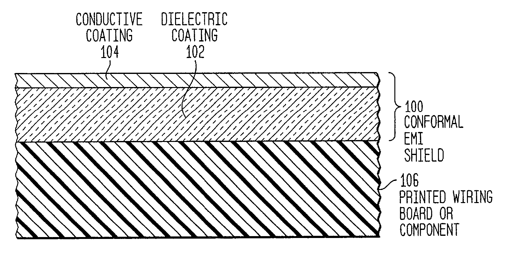
[0051] 2. Conformal EMI Shield Materials

[0052] A. Overview

[0053] B. Dielectric Coating

[0054] C. Conductive Coating

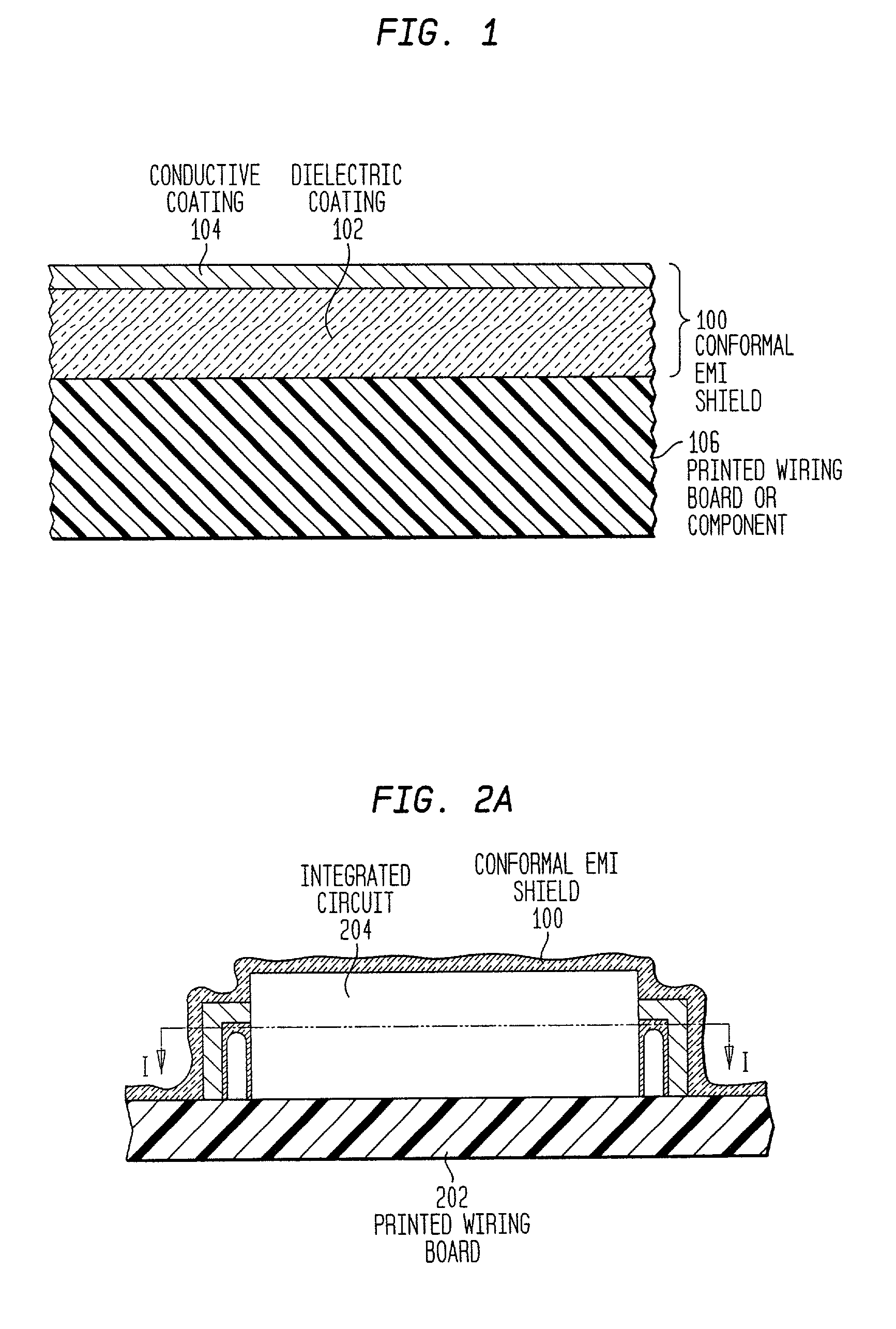
[0055] 3. A Printed Circuit Board With A Conformal EMI Shield

[0056] A. General

[0057] B. Printed Circuit Board Coverage

[0058] C. Grounding of Conformal EMI Shield

[0059] D. Electrically Connecting EMI Shielded Regions

[0060] E. Design of Printed Wiring Board to Accommodate EMI Shield

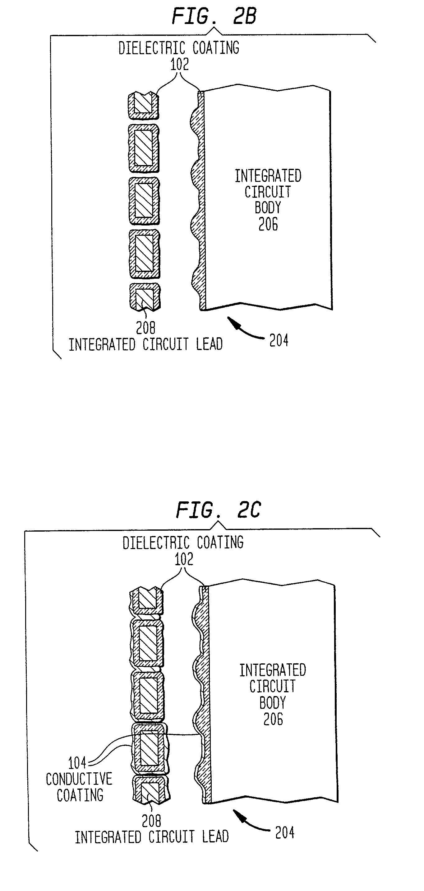
[0061] 4. Individual Components Coated with Conformal EMI Shield

[0062] 5. A Low Profile Component Cover For Encasing Components

[0063] 6. Filler Material For Use With Board-Level Containment of Electromagnetic Emissions

[0064] 7. Manufacturing of Printed Circuit Board With Conformal EMI Shield

[0065] 8. Closing

[0066] 1. Introduction

[0067] The present invention is directed to an electrically continuous conformal EMI protective shield and methods for applying same directly to the surfaces of one or more regions of a printed circuit board. When the EMI shi...


PUM

PropertyMeasurementUnit
thickaaaaaaaaaa
thickaaaaaaaaaa
thicknessaaaaaaaaaa

Abstract

An electrically continuous, grounded conformal EMI protective shield and methods for applying same directly to the surfaces of a printed circuit board. The EMI shield adheres and conforms to the surface of the components and printed wiring board. The shield takes the shape of the covered surfaces while adding little to the dimensions of the surfaces. The EMI shield includes low viscosity, high adherence conductive and dielectric coatings each of which can be applied in one or more layers using conventional spray techniques. The conductive coating prevents substantially all electromagnetic emissions generated by the shielded components from emanating beyond the conformal coating. The dielectric coating is initially applied to selected locations of the printed circuit board so as to be interposed between the conductive coating and the printed circuit board, preventing the conductive coating from electrically contacting selected components and printed wiring board regions. A high viscosity, non-electrically-conductive filler material is applied to printed circuit board regions that have surfaces that are cavitatious and/or which have a highly variable slope. The filler material can be used in conjunction with conformal EMI shield board level coating. The high viscosity, electrically non-conductive filler material substantially covers each cavity such that the covered cavity is inaccessible and that the covered region of the printed circuit board has a contiguous, contoured surface. A pre-manufactured non-electrically-conductive component cover can be mounted over a corresponding component and secured to the printed wiring board. The component cover and printed wiring board surround the component, forming a sealed enclosure. The component cover has a thin cross-section and an interior surface that follows closely the surface of the component. This minimizes the volume enclosed by the component cover. In addition, the exterior surface of the component cover has a low profile, and prevents the conformal EMI shield from physically contacting the covered component. Instead, the exterior surface of the component cover is coated with the EMI shield. This enables the covered component to be removed from the printed circuit board for repair, replacement or salvage without having to risk damage to the printed wiring board or component that may occur with the removal of a conformal EMI shield applied directly to the component.

Description

RELATED APPLICATIONS[0001] The present application is related to the following commonly owned U.S. Patent Applications:[0002] U.S. Patent Application entitled "FILLER MATERIAL AND PRETREATMENT OF PRINTED CIRCUIT BOARD COMPONENTS TO FACILITATE APPLICATION OF A CONFORMAL EMI SHIELD," naming as inventor Lowell E. Kolb and filed concurrently herewith under Attorney Docket No. 10001844-1; and[0003] U.S. Patent Application entitled "A LOW PROFILE NON-ELECTRICALLY-CONDUCTIVE COMPONENT COVER FOR ENCASING CIRCUIT BOARD COMPONENTS TO PREVENT DIRECT CONTACT OF A CONFORMAL EMI SHIELD," naming as inventor Lowell E. Kolb and filed concurrently herewith under Attorney Docket No. 10010907-1.BACKGROUND OF THE INVENTION[0004] 1. Field of the Invention[0005] The present invention relates generally to electromagnetic interference (EMI) protective measures and, more particularly, EMI protective measures for printed circuit boards.[0006] 2. Related Art[0007] Most countries in the world have regulations t...

Claims


Application Information

Patent Timeline
Patent Type & Authority Applications(United States)
IPC IPC(8): H01L23/552H05K1/02H05K3/28H05K9/00
CPCH01L23/552H01L2924/3011H05K1/0218H05K3/284H05K9/0039H01L2924/0002H01L2924/00Y10T29/49146Y10T29/49155Y10T428/25Y10T29/4913
Inventor BABB, SAMUEL M.KOLB, LOWELL E.DAVIS, BRIANMANKIN, JONATHAN P.MANN, KRISTINA L.MAZURKIEWICZ, PAUL H.WAHLEN, MARVIN
Owner HEWLETT PACKARD DEV CO LP
Why Eureka
Try Eureka