Double-gate field-effect transistor, integrated circuit using the transistor and method of manufacturing the same

a field-effect transistor and double-gate technology, applied in the direction of transistors, semiconductor devices, electrical devices, etc., can solve the problems of short channel effect, source and drain region, and inability to form two gate electrodes in alignment with the channel, so as to achieve suppress the effect of short channel

Inactive Publication Date: 2002-09-19
NAT INST OF ADVANCED IND SCI & TECH
View PDF0 Cites 73 Cited by
  • Summary
  • Abstract
  • Description
  • Claims
  • Application Information

AI Technical Summary

Benefits of technology

0016] Since the short channel effect can be suppressed by optimizing the electric potential at one of the two insulated gate electrodes, a sixth principal point of the present invention is to o

Problems solved by technology

Misalignment increases parasitic capacitance and resistance that, together with the fluctuations thereof, can lead to a marked degradation in device performance.
With the structure of the conventional double-gate field-effect transistor in which the vertically arranged gate electrodes, separated by the channel region, together with the source and drain regions, are not provided on the same principal surface, self-alignment cannot be employed, making it difficult to form the two gate electrodes in alignment with the channel, source and drain regions.
It has therefore been necessary to utilize the availabl

Method used


Image

  • Double-gate field-effect transistor, integrated circuit using the transistor and method of manufacturing the same
  • Double-gate field-effect transistor, integrated circuit using the transistor and method of manufacturing the same
  • Double-gate field-effect transistor, integrated circuit using the transistor and method of manufacturing the same

Examples


example 1

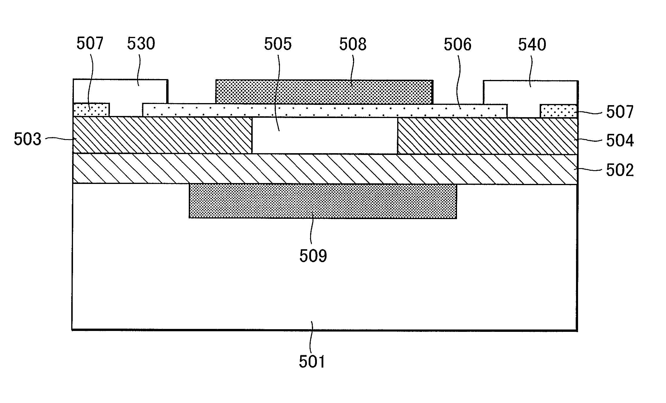
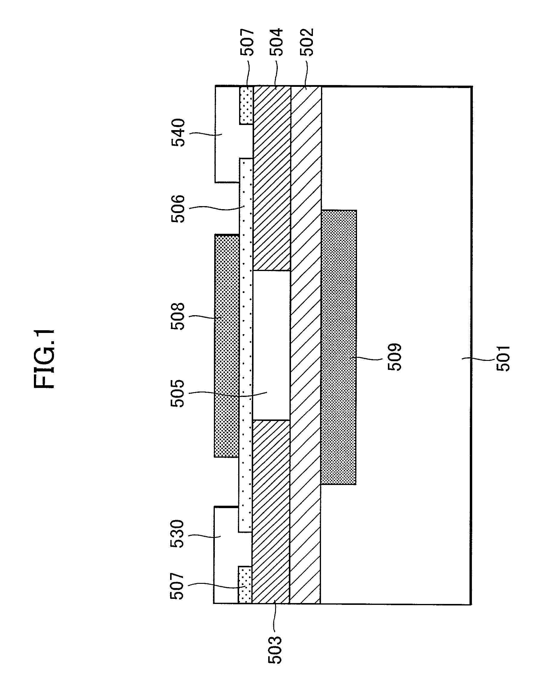
[0057] The sequence of steps comprising this procedure is shown in FIGS. 4 to 15. First, as shown in FIG. 4, a silicon oxide insulation film 2 is formed on a silicon substrate 1, and the silicon thus formed is used to provide a semiconductor crystal layer 3, followed by a silicon oxide film 4 and a silicon nitride film 5, in that order. Next, with reference to FIGS. 5 and 6, part of the silicon nitride film 5, silicon oxide film 4 and semiconductor crystal layer 3 is removed to form a trench 6 that isolates a layer island 200 from the surrounding portion. Here, the residual portion 100 is part of the semiconductor crystal layer 3, and silicon layer 31, silicon oxide film 41 and silicon nitride film 51 are the remaining parts of the semiconductor crystal layer 3, silicon oxide film 4 and silicon nitride film 5, respectively, that comprise the island 200.

[0058] As shown in FIG. 7, a silicon oxide film 22 is embedded in the trench 6 and is planarized by CMP or the like. FIG. 8 is a cro...

example 2

[0061] Another preferred embodiment of the method for manufacturing the double-gate field-effect transistor according to the present invention is shown in FIGS. 16 to 24. First, as shown in FIG. 16, a silicon oxide insulation film 2 is formed on a silicon substrate 1, and the silicon thus formed is used to provide a semiconductor crystal layer 3, on which are formed a silicon oxide film 4 and a silicon nitride film 5, in that order. Next, with reference to FIGS. 17 and 18, part of the silicon nitride film 5, silicon oxide film 4 and semiconductor crystal layer 3 is removed to form a trench 6 that isolates a layer island 200 from the surrounding portion. Here, the residual portion 100 is part of the semiconductor crystal layer 3, and silicon layer 31, silicon oxide film 41 and silicon nitride film 51 are the remaining parts of the semiconductor crystal layer 3, silicon oxide film 4 and silicon nitride film 5, respectively, that comprise the island 200. Up to this point, the process m...

example 3

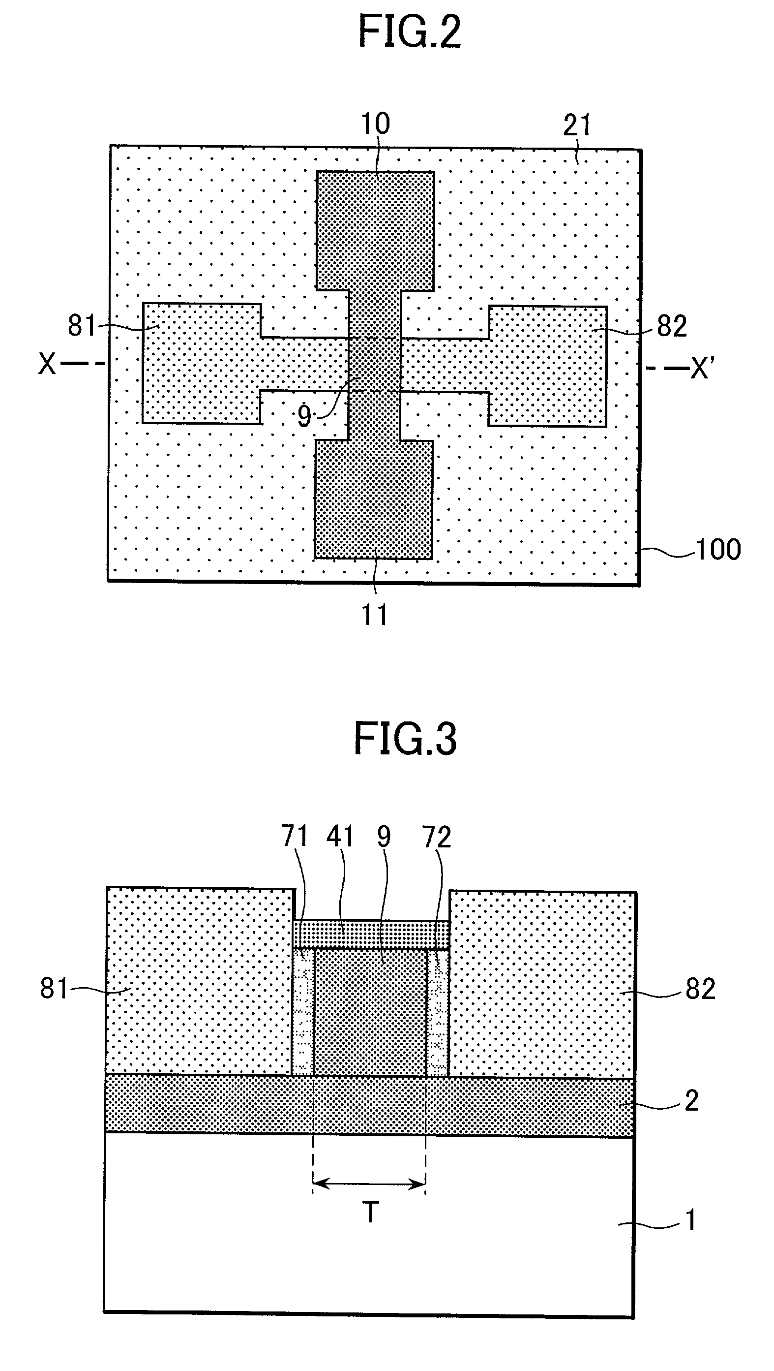
[0069] An example of a double-gate field-effect transistor comprising another embodiment of the invention will now be described. In this transistor, the width of the channel region is further decreased, enabling a marked suppression of the short channel effect. If the channel region is made thin enough, the result is a fully-depleted type transistor, making it possible to improve the transistor characteristics. FIG. 25 shows a plan view of the double-gate field-effect transistor with the reduced-width channel region, and FIG. 26 shows a cross-sectional view.

[0070] The steps of manufacturing the transistor shown in FIGS. 25 and 26 are shown in FIGS. 27 and 28. After achieving the shape shown, with reference to Example 2, in FIG. 23, polycrystalline silicon layers 18 and 19 are removed to form the trenches 16 and 17 of FIG. 27. FIG. 28 is a cross-sectional view along line X-X' of FIG. 27. Silicon oxide films 7-1 and 7-2 are removed from the side faces of the exposed channel region 9 s...


PUM


Abstract

A double-gate field-effect transistor includes a substrate, an insulation film formed on the substrate, source, drain and channel regions formed on the insulation film from a semiconductor crystal layer, and two insulated gate electrodes electrically insulated from each other. The gate electrodes are formed opposite each other on the same principal surface as the channel region, with the channel region between the electrodes. The source, drain and channel regions are isolated from the surrounding part by a trench, forming an island. Gate insulation films are formed on the opposing side faces of the channel region exposed in the trench. The island region between the gate electrodes is given a width that is less than the length of the channel region to enhance the short channel effect suppressive property of structure.

Description

BACKGROUND OF THE INVENTION[0001] 1. Field of the Invention[0002] The present invention relates to an insulated-gate field-effect transistor having a suppressed short channel effect, particularly to a double-gate field-effect transistor, and to an integrated circuit employing the transistor and a method of manufacturing the transistor.[0003] 2. Description of the Prior Art[0004] In order to achieve insulated-gate field-effect transistors with shorter channel lengths, it is necessary to suppress the short channel effect (the threshold voltage roll-off that occurs when the channel length is shortened). The double-gate field-effect transistor disclosed by Japanese Patent No. 2,021,931 has a device structure for achieving that. FIG. 1 is a cross-sectional view of a conventional double-gate field-effect transistor.[0005] With reference to FIG. 1, the transistor includes a substrate 501, a lower gate insulation film 502, a source region 503, a drain region 504, a channel region 505, an up...

Claims


Application Information

Patent Timeline
IPC IPC(8): H01L21/336H01L29/423H01L29/786
CPCH01L29/42384H01L29/66545H01L29/66795H01L29/66818H01L29/785
Inventor SEKIGAWA, TOSHIHIROISHII, KENICHISUZUKI, EIICHI
Owner NAT INST OF ADVANCED IND SCI & TECH
Why Eureka
Try Eureka