
Element isolating method in semiconductor integrated circuit device, semiconductor integrated circuit device and manufacturing method thereof

a semiconductor integrated circuit and element isolating technology, applied in semiconductor devices, electrical devices, transistors, etc., can solve the problems of reducing the inability to use design resources in the existing logical circuit portion, and the reduction of the degree of integration, so as to achieve finer nonvolatile memory size, no deterioration, and no impact on manufacturing margin

Inactive Publication Date: 2002-09-19
NEC ELECTRONICS CORP
View PDF0 Cites 10 Cited by
  • Summary
  • Abstract
  • Description
  • Claims
  • Application Information

AI Technical Summary

Benefits of technology

[0034] In view of the aforementioned problems, it is an object of the present invention to provide an element isolating method in a semiconductor integrated circuit device which involves no deterioration of performance of transistors for a nonvolatile memory or logical circuits, maintains the existing design scheme in transistors for logical circuits, and allows a finer size of the nonvolatile memory or high voltage transistors without impairing a manufacturing margin.
[0036] With such a configuration, since it is possible to form field oxide films. comprising oxide films with desired thicknesses respectively in the region where the high voltage semiconductor elements are formed, the element isolating performance can be maintained even in the region requiring high withstand voltage. In addition, since a field oxide film in a low voltage semiconductor element such as a transistor for a logical circuit can be set to have the existing thickness, the element isolating steps need not be changed and a reduced degree of integration can be prevented, thereby allowing the existing manufacturing process and existing design resources to be utilized. Moreover, the positions of respective element isolating areas are determined by the positions of the simultaneously formed second isolating trenches, and the increased number of lower components causes no increase in misalignment of masks for exposure. Thus, a smaller manufacturing margin can be prevented.
[0038] With this configuration, it is possible to significantly enhance withstand voltage for isolation between semiconductor elements as compared with the case where only the oxide film is provided, and predetermined element isolating performance can be obtained even with a thinner oxide film formed in the element isolating area.

Problems solved by technology

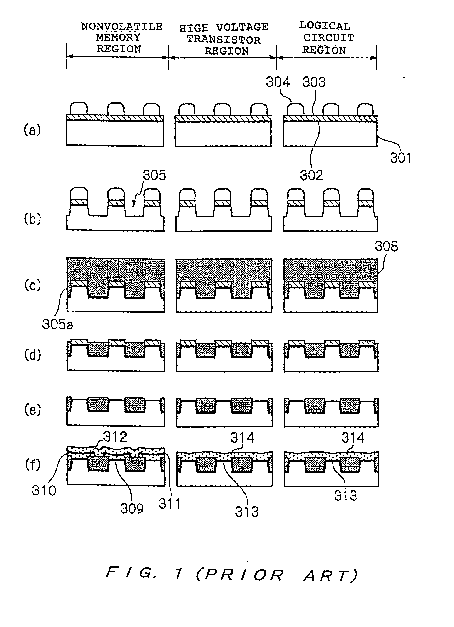
This causes the problem of a reduced degree of integration in the logical circuit region and the problem of the inability to use design resources in the existing logical circuit portion.
This leads to an increased area occupied by the nonvolatile memory region and the high voltage transistor region to cause the problem of a reduced degree of integration.
This approach, however, inevitably involves deteriorated performance of the nonvolatile memory due to an increase in time for writing data to and erasing data from a memory cell.
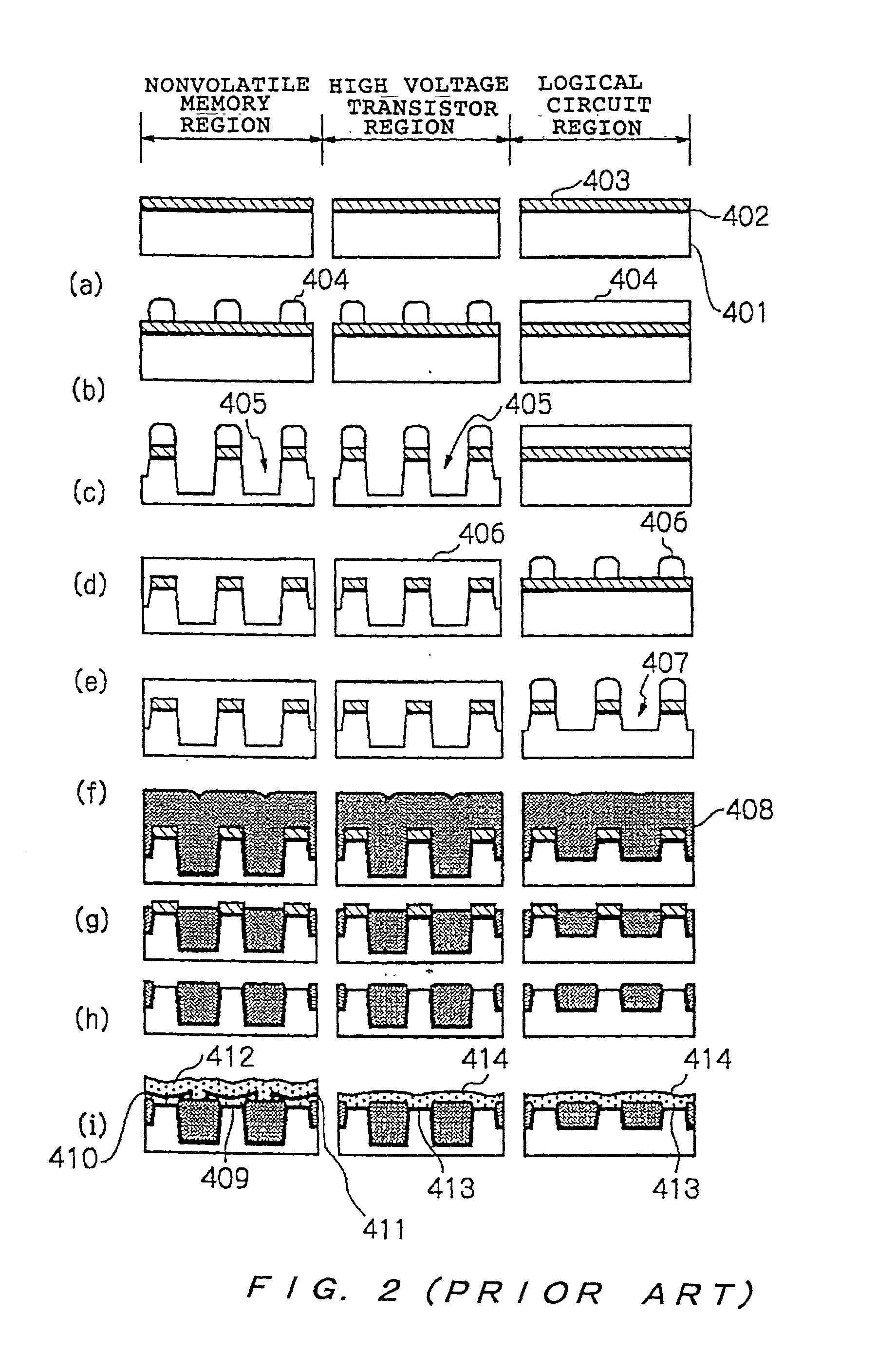
On the other hand, in the element isolating method of the second prior art, the formation of two lower components on a single Si substrate increases misalignment of masks for exposure, and particularly, the problem of a significantly smaller manufacturing margin (margin for misalignment) occurs at the formation of an upper component (for example, a contact for connecting a wiring pattern with an electrode for a transistor).
When the contacts in the two regions are individually formed to avoid the overlap between contact 417 and control gate electrode 412, a poor connection may occur between upper electrode 418 serving as wiring formed on interlayer insulating film 416 and contact 417 to result in an increased rate of occurrence of defective products at the manufacturing.

Method used


Image

  • Element isolating method in semiconductor integrated circuit device, semiconductor integrated circuit device and manufacturing method thereof
  • Element isolating method in semiconductor integrated circuit device, semiconductor integrated circuit device and manufacturing method thereof
  • Element isolating method in semiconductor integrated circuit device, semiconductor integrated circuit device and manufacturing method thereof

Examples


first embodiment

[0046] (First Embodiment)

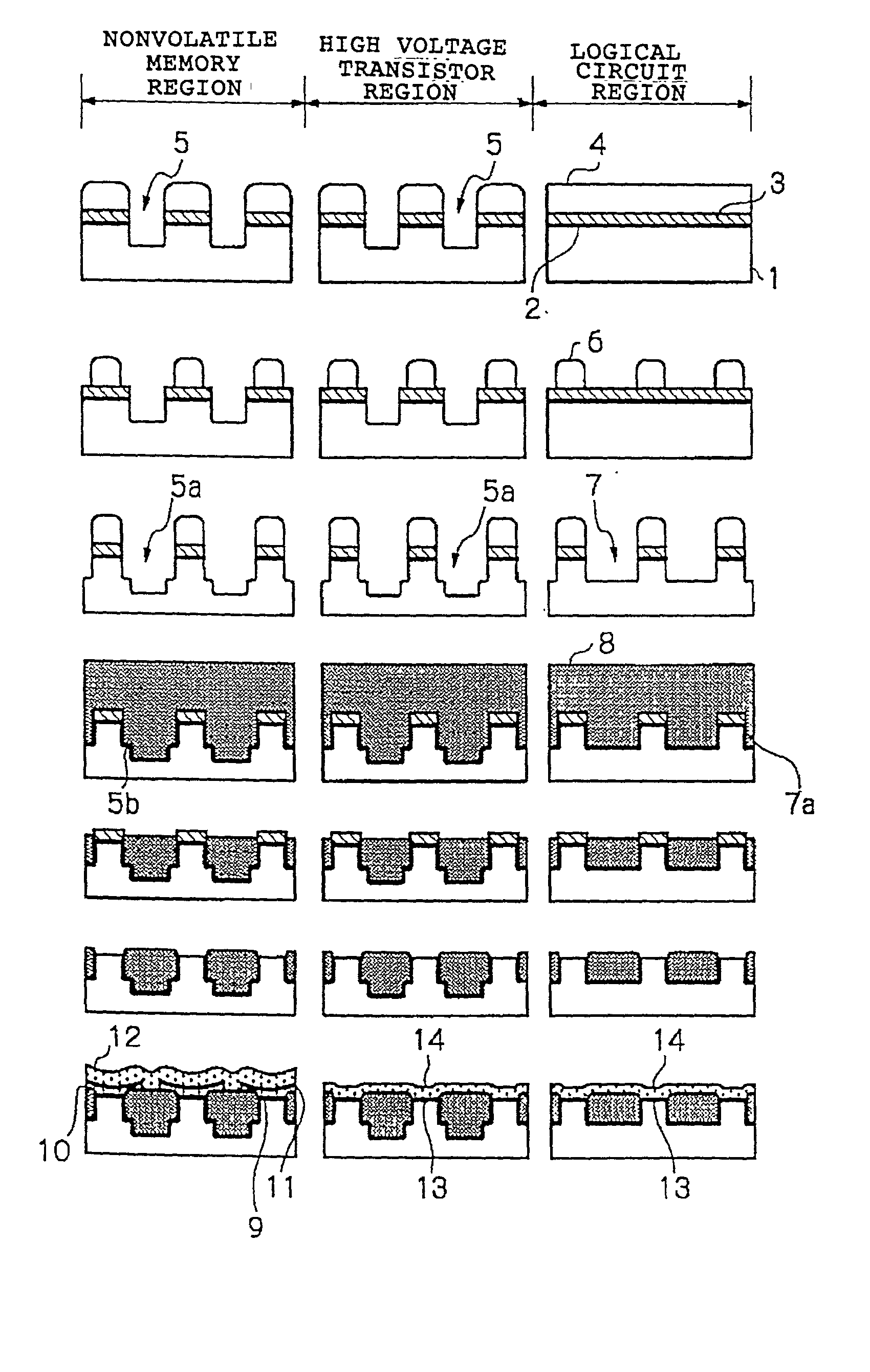
[0047] A first embodiment of an element isolating method in a semiconductor integrated circuit device according to the present invention is hereinafter described with reference to FIG. 5.

[0048] As shown in FIG. 5, in the first embodiment, silicon oxide film 2 with a thickness of approximately 10 nm is first deposited on Si substrate 1, and silicon nitride film 3 with a thickness of approximately 150 nm is deposited thereon. Subsequently, first photoresist 4 is deposited on silicon nitride film 3, and first photoresist 4 is patterned in order to form isolating trenches with a depth required for a nonvolatile memory region and a high voltage transistor region using a photolithography technique. First photoresist 4 is patterned to form the openings of a smaller width than a desired element isolating width. For example, when a desired element isolating width is 0.5 .mu.m, the openings are formed with a width of approximately 0.3 .mu.m.

[0049] Next, the parts of s...

second embodiment

[0059] (Second Embodiment)

[0060] Next, a second embodiment of the element isolating method in a semiconductor integrated circuit device according to the embodiment is described with reference to FIG. 6.

[0061] The element isolating method in a semiconductor integrated circuit device of the embodiment is an approach preferable for use in element isolation in a nonvolatile memory region and a high voltage transistor region which require high withstand voltage, in which polysilicon films serving as electrodes are embedded in isolating trenches provided in element isolating areas and a predetermined potential is applied to the polysilicon films to improve element isolating performance. The element isolating method of the embodiment may be used for a logical circuit region to which a normal power supply voltage is applied.

[0062] As shown in FIG. 6, in the second embodiment, silicon oxide film 102 with a thickness of approximately 10 nm is first deposited on Si substrate 101, and first pho...


PUM


Abstract

A first isolating trench with a predetermined depth is formed in a region where high voltage semiconductor elements are formed on a semiconductor substrate, and a portion of the walls of the first isolating trench is etched corresponding to a depth of a second isolating trench shallower than the first isolating trench to form a third isolating trench. An oxide film filled into the third isolating trench provides isolation between the high voltage semiconductor elements. Then, the second isolating trench is formed in a region where low voltage semiconductor elements are formed, and an oxide film filled into the second isolating trench is used to provide isolation between the low voltage semiconductor elements.

Description

BACKGROUND OF THE INVENTION[0001] 1. Field of the Invention[0002] The present invention relates to an element isolating method for providing isolation between elements mounted in a semiconductor integrated circuit device, and more particularly to an element isolating method in a semiconductor integrated circuit device in which a semiconductor element such as a nonvolatile memory to which a high voltage is applied and a semiconductor element such as a logical circuit to which a low voltage is applied are mounted together.[0003] 2. Description of the Related Art[0004] A semiconductor integrated circuit device in recent years does not have features such as a CPU, logical circuit and memory as individual units, but a tendency is accelerated toward SOC (System On Chip) in which those features are mounted on a single chip to constitute one system.[0005] As a memory mounted on such a semiconductor integrated circuit device, a flash EEPROM (Electrically Erasable Programmable Read-Only Memor...

Claims


Application Information

Patent Timeline
IPC IPC(8): H01L21/762H01L21/8247H01L27/10H01L21/76
CPCH01L21/76229H01L27/11526H01L27/11546H10B41/49H10B41/40H01L27/10
Inventor SHIMIZU, MASAKUNIIO, EIJI
Owner NEC ELECTRONICS CORP
Learn More