
Memory device search system and method

Inactive Publication Date: 2002-09-19
SHERMAN DAVID L
View PDF0 Cites 32 Cited by
  • Summary
  • Abstract
  • Description
  • Claims
  • Application Information

AI Technical Summary

Benefits of technology

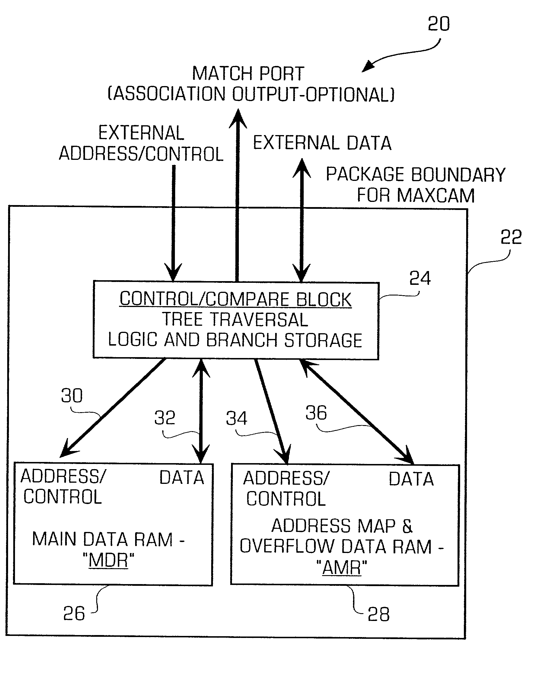
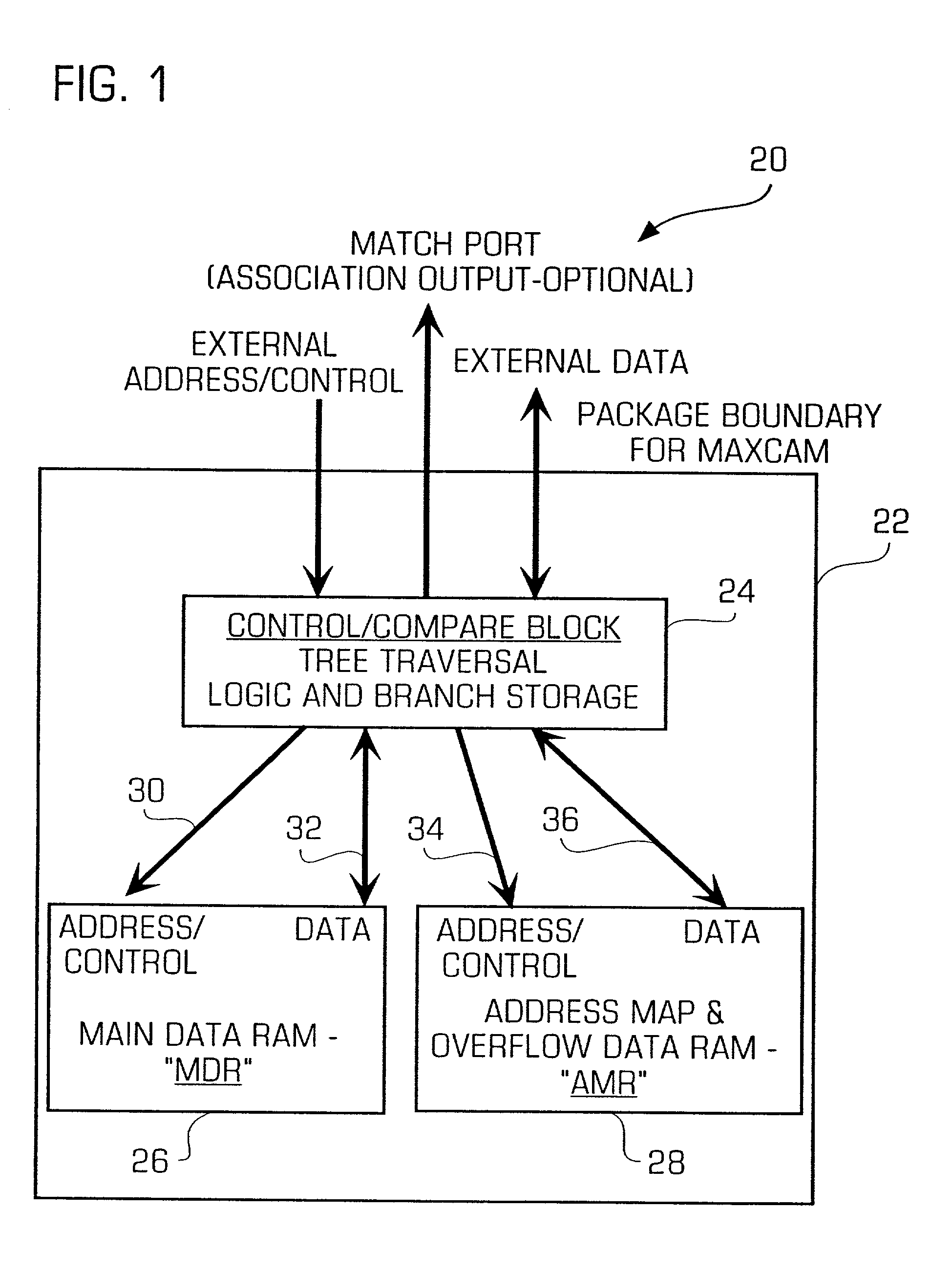
[0031] In accordance with the invention, the 2 DRAM blocks (MDR and AMR) may also be available as very fast ordinary RAM in which case the Controller / Comparer 24 may configure the CAM to allocate anywhere from 0-100% of the DRAM memory locations to the CAM and the remainder to the RAM operation. Even with the allocation of memory locations, the system still permits RAM-style accesses to the part being used (mapped) to the CAM operation. For the memory locations being used for strictly RAM operations typical full speed burst operations may be available. This allows the CAM to be used in DIMM sockets in servers that permits an easy upgrade path for use in list processing and data manipulation tasks in servers. Now, details of the search architecture and method in accordance with the invention will be described.
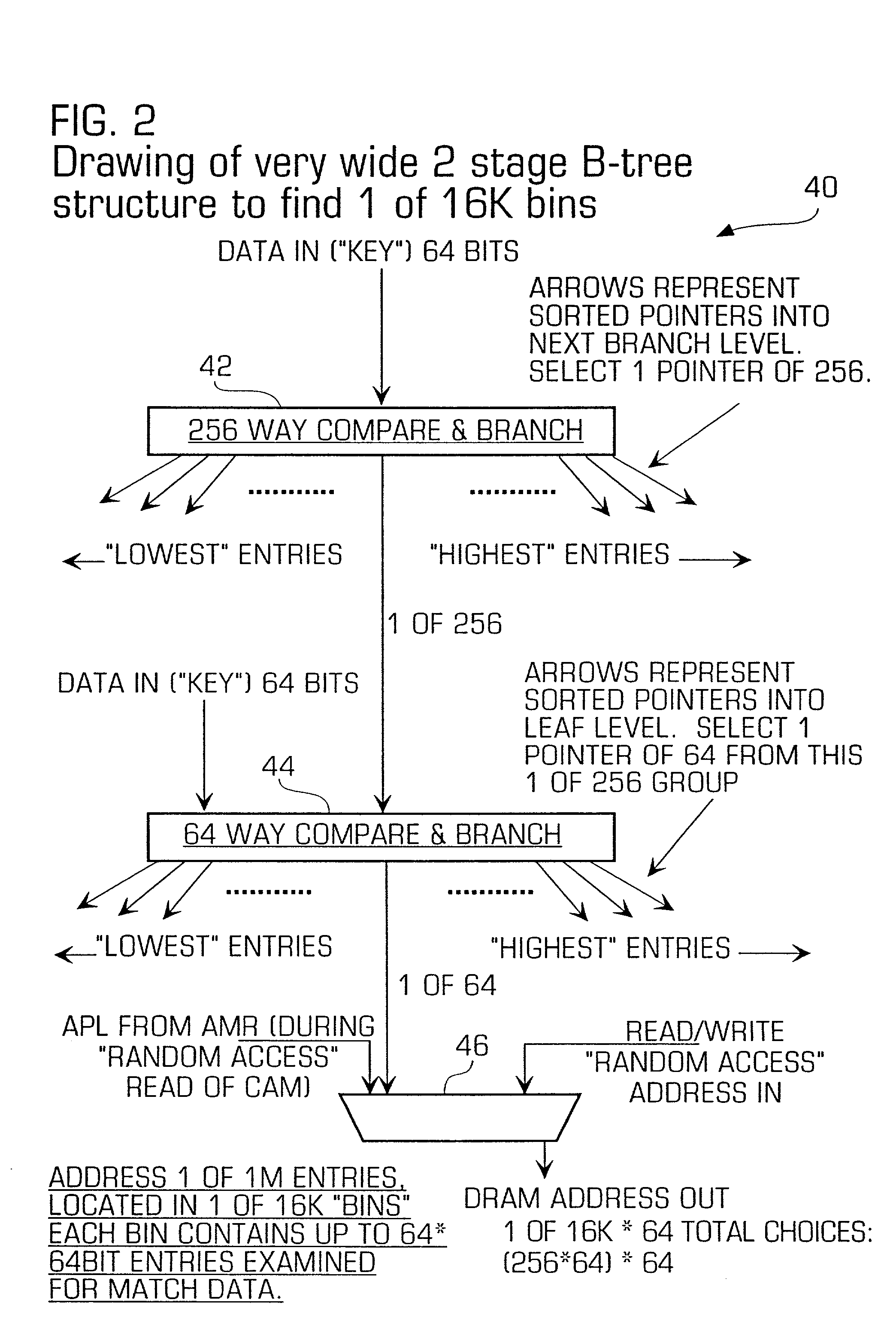
[0032] FIG. 2 is a diagram illustrating the searching architecture 40 in accordance with the invention that permits a more rapid searching of the contents of the CAM in accordance with the invention. In accordance with the invention, a very wide search tree as described below may be used in order to converge on a data match in a tree structure rapidly. A very wide search tree is also more economical with branching between 64 and 1024 ways at each level, depending on the size of the ultimate DRAM that contains the leaves. In this preferred embodiment of a 1M*64 CAM architecture, there is a 2 level B-tree structure that finds an index into a final "bin" or "leaf" which contains 64 entries in a DRAM. The 64 entries may then be fetched by address (i.e., the index is retrieved from the b-tree structure) and compared against the key so that the comparison occurs with only the 64 entries instead of all of the entries which significantly reduces the comparison time of the CAM in accordance with the invention. In the architecture, note that there is no "CAM-cell" memory structure in the large memory blocks, only SRAM and DRAM memory cells.
[0033] Returning to FIG. 2, the architecture 40 may receive input data (a "key") that may be 64 bits in the example of the preferred embodiment. In accordance with the invention, the key may be fed into a 256 way compare and branch logic 42 that compares the key to each of 256 groups of the memory to generate a single pointer to the next branch level. The pointer generated by this logic 42 may be fed into a 64 way compare and branch logic 44 which also is fed the key. This logic 44 may again compare the key to each of 64 groups within the selected group from the original 256 to generate a single selected memory pointer to a block of memory. In this manner, the number of full memory locations that are compared to the entire key is rapidly reduced so that the final comparison of the full key to memory locations may be completed rapidly. The structure of the compare and branch logic 42, 44 is further illustrated in FIG. 7.

Problems solved by technology

The key problems with typical CAMs is that compare logic, that performs the comparison of the desired data to each memory location in the CAM, must be located at every memory cell location which significantly increases the number of transistors that must be dedicated to the compare logic and correspondingly decreases the amount of storage the CAM (since fewer transistors may be used for storage) assuming a fixed number of transistors on an integrated circuit.
In addition, there is a large amount of power dissipation associated with every word having a dynamic match line that cycles during every compare operation.
These problems severely limit the potential size of the CAM both in terms of the silicon area and not being able to economically package the die due to the heat generated.

Method used


Image

  • Memory device search system and method
  • Memory device search system and method
  • Memory device search system and method

Examples


Embodiment Construction

[0025] The invention is particularly applicable to a 64 Mbit content addressable memory (CAM) device that uses 128 Mb of DRAM and it is in this context that the invention will be described. It will be appreciated, however, that the system and method in accordance with the invention has greater utility, such as to other types of memory devices that may use other types of typical memory blocks such as SRAM or Embedded DRAM. In addition, the invention may be implemented on a single silicon die or as several die in a multi-chip package. It will be appreciated that this architecture achieves the same advantages over traditional CAM in subsequent memory density generations. Now, the preferred embodiment of the invention implemented as a CAM will be described.

[0026] FIG. 1 is a block diagram illustrating a preferred embodiment of a single die content addressable memory (CAM) 20 in accordance with the invention that implements the search architecture in accordance with the invention. The CA...


PUM


Abstract

A search system and method is provided that may implemented in a content addressable memory (CAM) using various different memory technologies including SRAMs. DRAMs or Embedded DRAMs. The search system increases the density and efficiency of the CAM by using a search tree to reduce the total number of entries that must be matched against the key.

Description

[0001] This invention relates generally to a system and method for performing rapid searches in a memory and in particular to a searching method and system for a content addressable memory device that permits rapid searches to be performed for data contained in the memory.[0002] A content addressable memory (CAM) device is a memory storage device that accelerates any application that requires fast searches of data stored in the memory. For example, searching a database, a list, or for a particular pattern in database machines, image or voice recognition or computer and communication networks may be particularly well suited to using a CAM. A CAM operates by simultaneously comparing the desired information provided by the user against a list of pre-stored entries. The CAM gives an order of magnitude reduction in search time as compared to a typical random access memory (RAM).[0003] A RAM is an integrated circuit that temporarily stores data. The data is stored in various different sto...

Claims


Application Information

Patent Timeline
IPC IPC(8): G06F7/06G06F12/00H04L12/56
CPCH04L45/7453H04L49/90Y10S707/99936
Inventor SHERMAN, DAVID L.
Owner SHERMAN DAVID L
Learn More