Two-stage multiplier circuit

a multiplier circuit and circuit technology, applied in the field of network interfaces, can solve the problems of relatively unstable operation of conventional systems employing present techniques, relatively high data rate communication circuits, and relatively high cost of implementation or operation of conventional circuits

Inactive Publication Date: 2002-09-26
CONNECTCOM MICROSYST
View PDF6 Cites 3 Cited by
  • Summary
  • Abstract
  • Description
  • Claims
  • Application Information

AI Technical Summary

Problems solved by technology

Conventional circuits for communicating data at very high data rates have proven inadequate.
Conventional circuits are relatively expensive to implement or are relatively slow in operation.
Further, conventional systems employing present techniques are often relatively unstable in operation and are difficult to integrate with other systems.
In addition, conventional circuits inefficiently consume relatively large amounts of power, thereby wasting power, requiring expensive circuit packaging, and increasing heat dissipation requirements.
Due to the inadequacies of the present art, users have had to pay for expensive network interfaces or have suffered from the frustration and the wasted time associated with low-speed systems.
By contrast, a line test disadvantageously fails to test a significant portion of a transceiver 300.
Although the diagnostic test tests a relatively large portion of the transceiver 300, implementation of the diagnostic test disadvantageously requires a relatively large array of relatively expensive test equipment.
By contrast, conventional circuits sample the transition of the data period with relatively n

Method used


Image

  • Two-stage multiplier circuit
  • Two-stage multiplier circuit
  • Two-stage multiplier circuit

Examples


Embodiment Construction

Incorporation by Reference of Commonly Owned Applications

[0402] The following patent applications, commonly owned and filed on the same day as the present application, are hereby incorporated herein in their entirety by reference thereto:

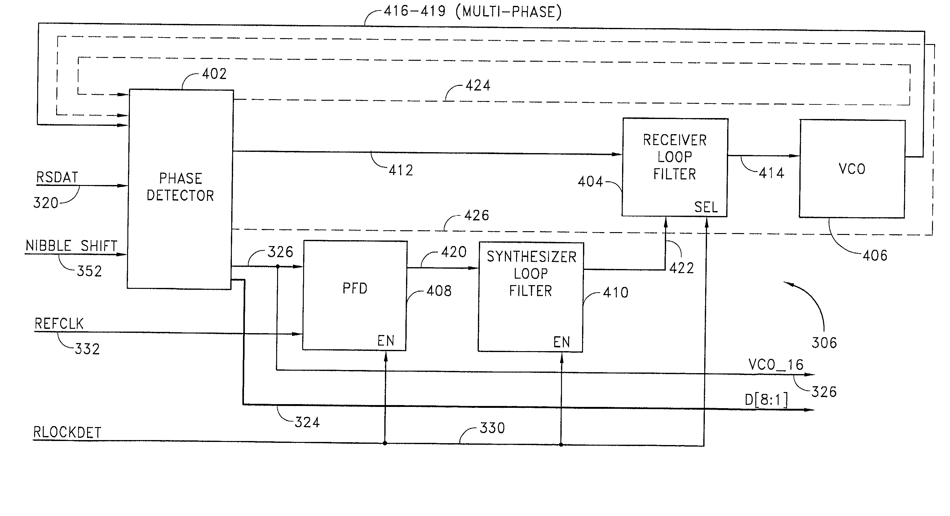
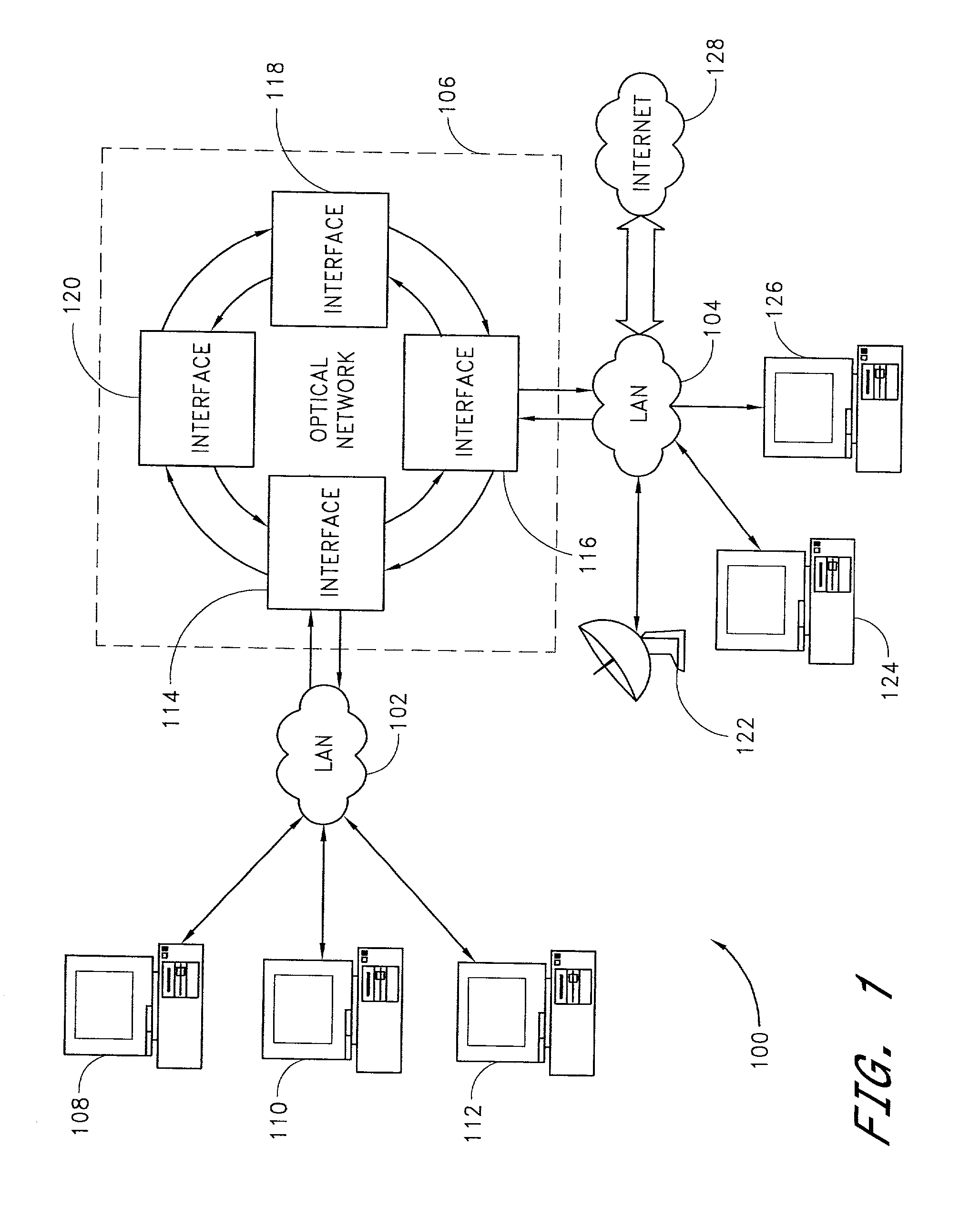
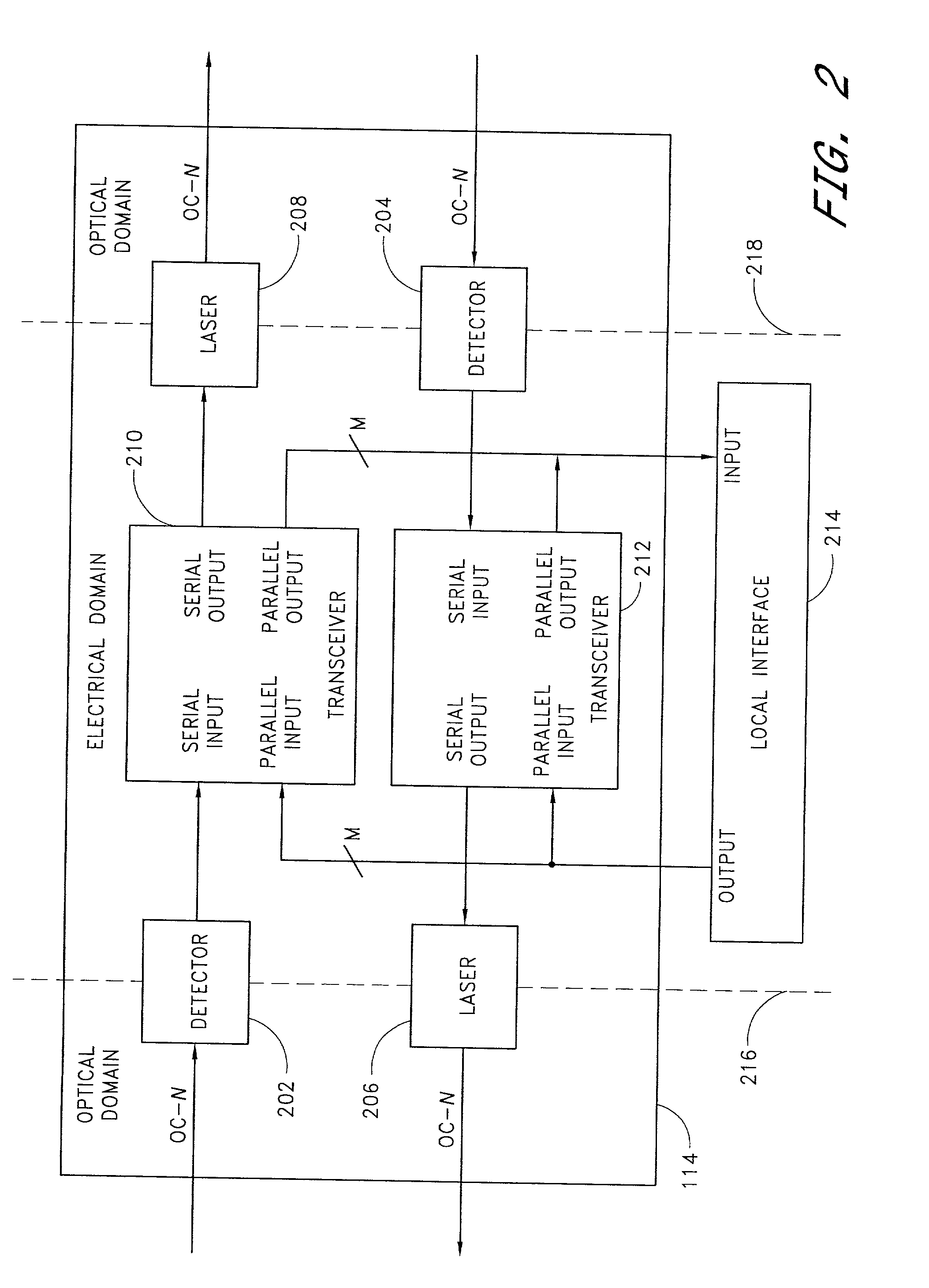
9 Application Attorney Title No. Docket No. "Integration and Hold Phase Detection" CCOM.003A "Current Mode Phase Detection" CCOM.004A "Trigger Circuit" CCOM.005A "Reset Circuit" CCOM.007A "Multiplier Circuit" CCOM.008A "Data Transition Identifier" CCOM.009A "Frame Pattern Detection in an Optical CCOM.016A Receiver" "Single to Differential Input Buffer CCOM.017A Circuit" "Acquisition Aid Circuit" CCOM.018A "Low Voltage Differential Signaling CCOM.019A Output Buffer" "Low Frequency Loop-Back in a High- CCOM.020A Speed Optical Transceiver" "Phase Frequency Detector" CCOM.021A "Phase Alignment of Data to Clock" CCOM.022A "Voltage Controlled Oscillator" CCOM.023A "System and Method of Digital Tuning a CCOM.024A Voltage Controlled Oscillator" "System and ...


PUM


Abstract

The invention relates to methods and apparatus that receive an integration result, receive logic states of data bits corresponding to the integration result, and perform a high-speed multiplication operation. Embodiments of the invention selectively multiply the integration result according to the logic states of the corresponding data bits. Advantageously, relatively large integration results corresponding to data bit transitions that do not include a change of logic states, such as logic 0 to logic 0 or logic 1 to logic 1, can be multiplied by zero (0). Relatively smaller integration results corresponding to integrations of data bit transitions including a change in logic states, such as from logic 0 to logic 1 or from logic 1 to logic 0, can be multiplied by one (1) and by negative one (-1).

Description

PRIORITY CLAIMS[0001] The benefit under 35 USC. .sctn.119(e) of U.S. Provisional Application No. 60 / 208,899, filed Jun. 2, 2000, and entitled "MIXED MODE TRANSITIVE" and of U.S. Provisional Application No. 60 / 267,366, filed Feb. 7, 2001, and entitled "TRANSITIVE," is hereby claimed.APPENDIX A[0002] Appendix A, which forms a part of this disclosure, is a list of commonly owned copending U.S. patent applications. Each one of the applications listed in Appendix A is hereby incorporated herein in its entirety by reference thereto.COPYRIGHT RIGHTS[0003] A portion of the disclosure of this patent document contains material that is subject to copyright protection. The copyright owner has no objection to the facsimile reproduction by anyone of the patent document or of the patent disclosure as it appears in the Patent and Trademark Office patent files or records, but otherwise reserves all copyright rights whatsoever.[0004] 1. Field of the Invention[0005] The invention generally relates to ...

Claims


Application Information

Patent Timeline
IPC IPC(8): H03D7/14H03H11/52H03K19/018H03L7/085H03L7/087H03L7/089H03L7/091H03L7/099H03L7/10H03L7/14H03L7/18H04J3/06H04L1/24H04L7/00H04L7/033H04L25/02H04L25/05
CPCH03D7/1433H03H11/52H03K19/01812H03L7/085H03L7/087H03L7/0896H03L7/091H03L7/099H03L7/10H03L7/14H03L7/18H03L2207/06H04J3/0608H04L1/242H04L7/0008H04L7/033H04L7/0337H04L7/0338H04L25/0266H04L25/0272H04L25/0274H04L25/0278H04L25/028H04L25/0282H04L25/0286H04L25/0292H04L25/0294H04L25/05H03D7/1441H03D7/1458H03D2200/0033H03D2200/0043H03D2200/0047H03F3/45085H03F2203/45592H03F2203/45612
Inventor ENAM, SYED K.DJAFARI, MASOUDSMYTHE, R. KENT
Owner CONNECTCOM MICROSYST
Why Eureka
Try Eureka