
Electronic device

Inactive Publication Date: 2002-09-26
CONTINENTAL AUTOMOTIVE GMBH
View PDF0 Cites 10 Cited by
  • Summary
  • Abstract
  • Description
  • Claims
  • Application Information

AI Technical Summary

Benefits of technology

[0009] The present invention has the advantage that the filter device is an integral component of the carrier substrate and can be prepared at the time the printed circuit board is manufactured. When the first and second conductor surfaces are installed in the device, the conductor surfaces only need to be connected to the electrical potentials. The position of the filter formed by the first and second conductor surfaces is permanently predefined by the installation position of the printed circuit board. The mounting procedure does not require any additional adjustment measures such as occur when separate filter devices are used. This has the advantage that a customary printed circuit board which has a plurality of conductor tracks lying one on top of the other acts itself as a filter device.
[0012] The filter device can thus easily be positioned at the location where experience has shown that the greatest incidence of interference radiation is to be expected, and prevents, when mounted in accordance with the specifications, the ingress of high frequency radiation into the interior of the housing. This results in a device which can be handled particularly satisfactorily for mass production.
[0015] In this way, a single pressing-in operation is effective for securing the plug a simultaneously making electrical contact with the capacitor electrode.
[0016] The use of a plug-in device with a plurality of plug-in elements makes it easily possible for the first capacitor surfaces, which are electrically insulated from one another and are associated with different plug-in elements, to be formed for each plug-in element in one conductor layer.
[0017] Such a structure can easily be manufactured during one operation when the printed circuit board is manufactured.
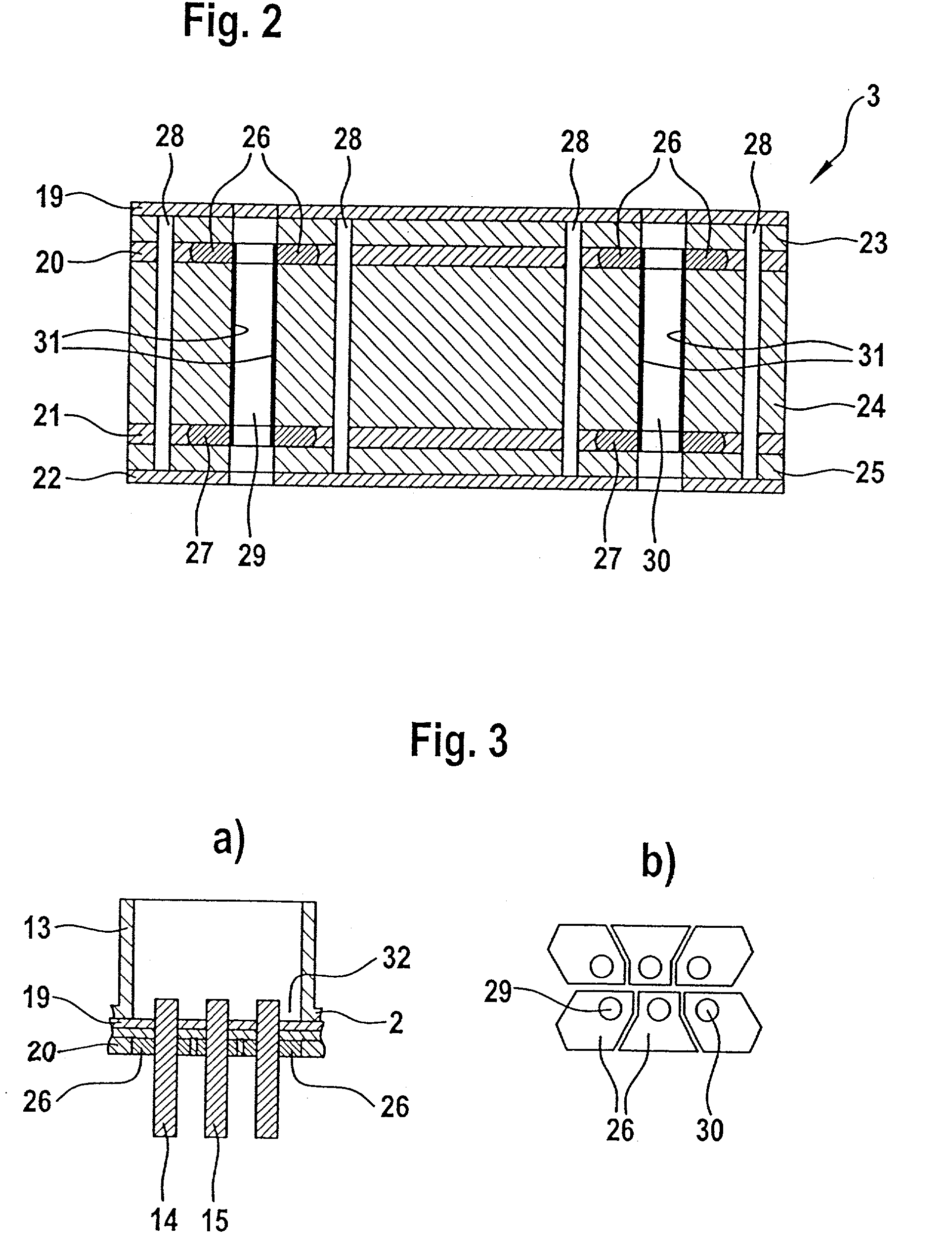
[0020] In one embodiment, the fourth conductor surface may also be implemented as an unstructured contact surface which is arranged on the second outer side of the carrier element, the unstructured contact surfaces which lie approximately one on top of the other are electrically connected to one another in the periphery of each plug-in element by a plurality of vias. As a result, a type of Faraday cage is formed around the plug-in element. That, along with the fact that an outer side of the carrier element bears tightly against the preferably electrically conductive housing, reliably prevents interference radiation from penetrating the interior of the housing.

Problems solved by technology

It is disadvantageous here that during the mounting of this planar filter, satisfactory functioning of the planar filter is ensured only if a reliable electrical and / or capacitive connection to the housing is ensured to avoid undefined capacitance values.

Method used


Image

  • Electronic device
  • Electronic device
  • Electronic device

Examples


Embodiment Construction

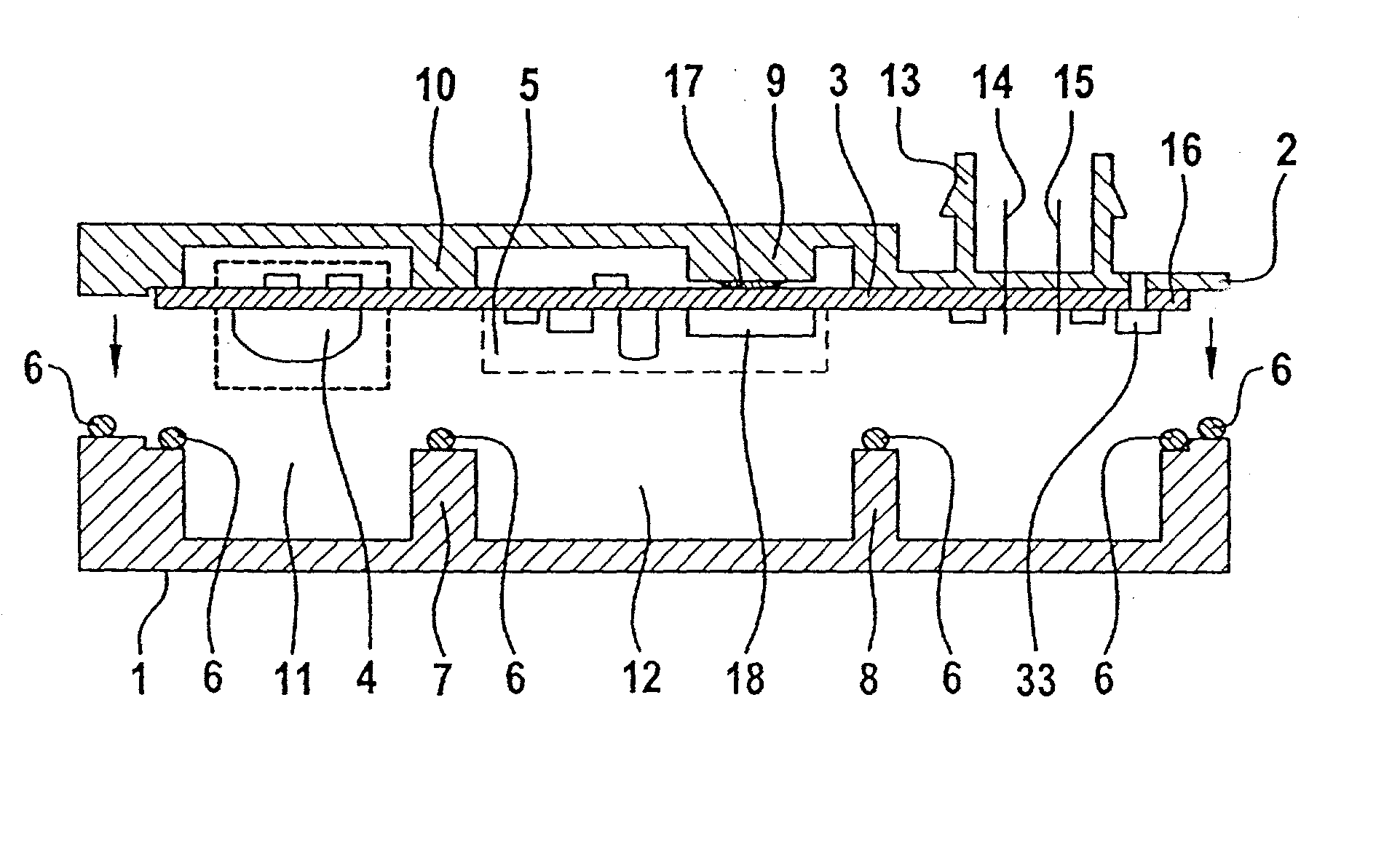
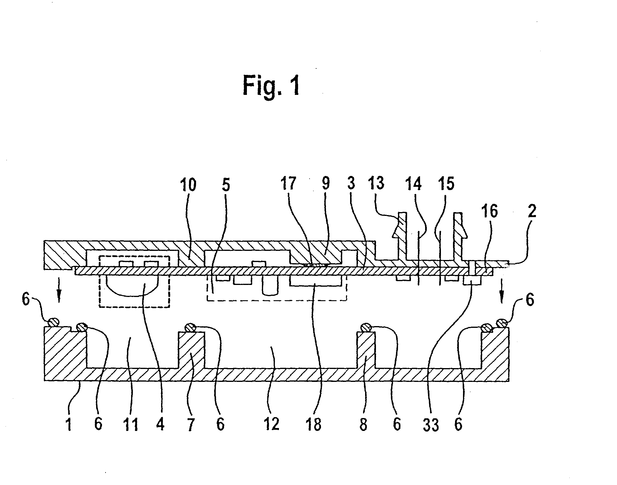
[0027] FIG. 1 illustrates an electrical device that is generally used in motor vehicles. This device may comprise a control device for a motor vehicle which has signal-processing electronics which are known to be very susceptible to high-frequency interference. However, the electronic device may also comprise a sensor device which has not only the actual sensor but also a signal-conditioning circuit and / or a signal-evaluation circuit which are arranged on one printed circuit board or a plurality of printed circuit boards.

[0028] The electronic device has an electrically conductive cup-shaped housing part 1 which is composed, for example, of aluminum and which is sealed off with a cover 2 which is also electrically conductive. A multilayer printed circuit board 3 is fitted with a sensor 4 and signal-conditioning electronics 5 for the sensor 4 and is arranged within the housing part 1. The housing part 1 and cover 2 are sealed with respect to one another by a conductive rubber seal 6. ...


PUM


Abstract

An electronic device includes a housing for accommodating a carrier substrate. An electronic module and a conductor structure for making electrical connection with the electronic module are fitted on the carrier substrate. A filter device for improving the electromagnetic sensitivity is arranged in the housing. The filter device is formed by an electrical and / or capacitive connection of a first conductor surface of the conductor structure to an external first potential and by an electrical and / or capacitive connection of a second conductor surface of the conductor structure to a second electrical potential, the first conductor surface and the second conductor surface being arranged approximately opposite one another.

Description

[0001] 1. Field of the Invention[0002] The invention relates to an electronic device having a housing for accommodating a carrier substrate and a filter device arranged in the housing for improving the electromagnetic sensitivity of the device, said carrier substrate being fitted with an electronic module and a conductor structure for making electrical connection with the electronic module.[0003] 2. Description of the Related Art[0004] Shielding electronic devices against interference radiation which occurs in the high frequency range is required to ensure satisfactory functioning of electronic devices. Such interference suppression measures are usually provided in the interior of the electronic device.[0005] German reference DE 299 02 505 U1 discloses a planar filter in which a capacitor is formed on a ceramic substrate. One side of the ceramic substrate is provided with the mass electrode and the other side with the signal electrodes of the capacitor. The signal electrodes form in...

Claims


Application Information

Patent Timeline
IPC IPC(8): H05K7/08H01R13/24H01R13/658H01R13/719H05K1/02H05K1/16H05K3/34H05K3/42H05K3/46H05K9/00
CPCH01R13/2414H01R13/65802H01R13/7195H05K1/0231H05K1/162H05K3/3447H05K3/429H05K3/4652H05K9/0018H05K2201/0191H05K2201/09672H05K2201/09809H05K2201/10189H01R13/6581H05K9/0066
Inventor BERBERICH, REINHOLD
Owner CONTINENTAL AUTOMOTIVE GMBH
Learn More