Surface emitting semiconductor laser device

a laser device and surface technology, applied in the direction of semiconductor laser excitation apparatus, laser details, excitation process/apparatus, etc., can solve the problems of reducing the peak intensity of photoluminescence (pl intensity), reducing the optical output of the surface emitting laser, and reducing the quantum efficiency

Inactive Publication Date: 2002-10-10
FURUKAWA ELECTRIC CO LTD
View PDF0 Cites 28 Cited by
  • Summary
  • Abstract
  • Description
  • Claims
  • Application Information

AI Technical Summary

Problems solved by technology

The nitrogen content as high as 0.5 to 1%, however, has a disadvantage in that the peak intensity of the photoluminescence (PL intensity) is lowered.
The rise of the operational voltage may be suppressed by doping the layers with impurities at a dosage of 1 .times.10.sup.18 to 5.times.10.sup.18 cm.sup.-3, which however significantly lowers the quantum efficiency due to absorption of free carriers by the impurities and thus reduces the optical output of the surface emitting laser.
The described combination laser, however, has a lower throughput for fabrication thereof due to the bonding process for the substrates, and thus is not suited for mass production of the surface emitting laser.

Method used


Image

  • Surface emitting semiconductor laser device
  • Surface emitting semiconductor laser device
  • Surface emitting semiconductor laser device

Examples


Embodiment Construction

[0035] Now, the present invention is more specifically described with reference to accompanying drawings.

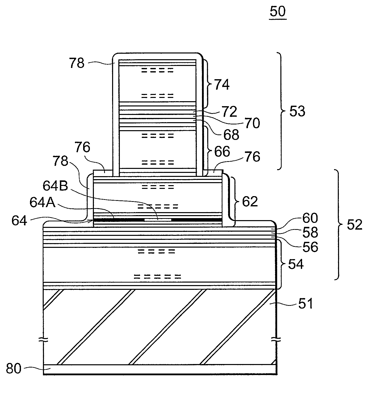
[0036] Referring to FIG. 3, a surface emitting laser according to an embodiment of the present invention is implemented as a combination laser including a pair of laser sections monolithically formed on a single GaAs substrate.

[0037] More specifically, the surface emitting laser of the present embodiment, generally designated by numeral 50, includes an n-type GaAs (n-GaAs) substrate 51, a first surface emitting laser section (first laser section) 52 formed on the n-GaAs substrate 51 and having an emission wavelength of 850 nm, and a second surface emitting laser section (second laser section) 53 formed on the first laser section 52 and having an emission wavelength of 1300 nm. The first laser section 52 has GaAs / AlGaAs-based layer structure, whereas the second laser section 53 includes a GaInNAs-based layer structure.

[0038] The first laser section 52 has a layer structure includi...


PUM


Abstract

A surface emitting semiconductor laser device includes a GaAs substrate, and first and second laser sections consecutively and monolithically formed on the GaAs substrate. The second laser section has an active layer structure having a bandgap wavelength longer than the bandgap wavelength of the active layer structure of the first laser section. The second laser section is pumped by a first laser emitted by the first laser section to emit second laser.

Description

[0001] 1. Field of the Invention[0002] The present invention relates to a long-wavelength surface emitting semiconductor laser device and, more particularly, to a long-wavelength surface emitting semiconductor laser device having a higher emission efficiency, an improved temperature characteristic and a longer lifetime.[0003] 2. Description of the Related Art[0004] A surface emitting semiconductor laser device (hereinafter referred to as simply "surface emitting laser") emits laser in the direction perpendicular to the main surface of the substrate and has an advantage over the conventional Fabry-Perot laser device in that a plurality of semiconductor laser devices can be arranged on a single substrate in a two-dimensional array. Thus, the surface emitting laser attracts a larger attention in the field of data communication in these days.[0005] The surface emitting laser includes a GaAs or InP substrate, a pair of multilayer reflecting mirrors (hereinafter referred to as DBR mirrors...

Claims


Application Information

Patent Timeline
Patent Type & Authority Applications(United States)
IPC IPC(8): H01S5/026H01S5/04H01S5/183H01S5/42
CPCB82Y20/00H01S5/0021H01S5/041H01S5/426H01S5/18344H01S5/34306H01S5/18311
Inventor IWAI, NORIHIRO
Owner FURUKAWA ELECTRIC CO LTD
Why Eureka
Try Eureka