Transparent conductive laminated body and touch panel

a technology of transparent conductive and laminated body, applied in the field of transparent conductive, can solve the problems of inferior flexibility and workability of conductive glass, decreased transparency, and inability to meet certain usag

Inactive Publication Date: 2002-10-31
NITTO DENKO CORP
View PDF2 Cites 139 Cited by
  • Summary
  • Abstract
  • Description
  • Claims
  • Application Information

AI Technical Summary

Problems solved by technology

As a conventional transparent conductive thin film, a so-called conductive glass in which indium oxide thin film is formed on a glass plate is known well, but since a substrate is made of glass, the conductive glass is inferior in flexibility and workability, and it is not suitable for a certain usage.
However, transparent conductive thin films using the film substrate have a problem that transparency is decreased because of a large light reflection factor on surface thereof, and also have a problem that electric resistance is increased or disconnection of circuits may occur because of blemish given while in use since the conductive thin film is inferior in scratch-proof property.
However, since an excellent dotting property was not realized in the transparent conductive thin films using the above described film substrate, the films had a problem that only a short life as a touch panel could be realized.
When the thickness is less than 2 .mu.m, insufficient mechanical strength as a substrate is obtained, and difficulty occurs in operation when a roll-shaped dielectric substance thin film, conductive thin film and pressure sensitive adhesive layer are continuously formed from this substrate.
In addition, since there is a possibility that improvement in transparency may not be expected and a crack may arise, an excessive thickness of the dielectric substance thin film 3 is not preferable.
Moreover, if the thickness of the pressure sensitive adhesive layer 5 is set to less than 1 .mu.m, since the cushioning effect is not expectable either, an improvement in the scratch-proof property of the conductivity thin film 4 or of the dotting property of as touch panels may not be expected.
If the thickness is excessive, transparency will be spoiled or a good result may not be realized in respect of formation of the pressure sensitive adhesive layer 5, and of workability in adhering of a transparent substrate, and cost.

Method used


Image

  • Transparent conductive laminated body and touch panel
  • Transparent conductive laminated body and touch panel

Examples


example 1

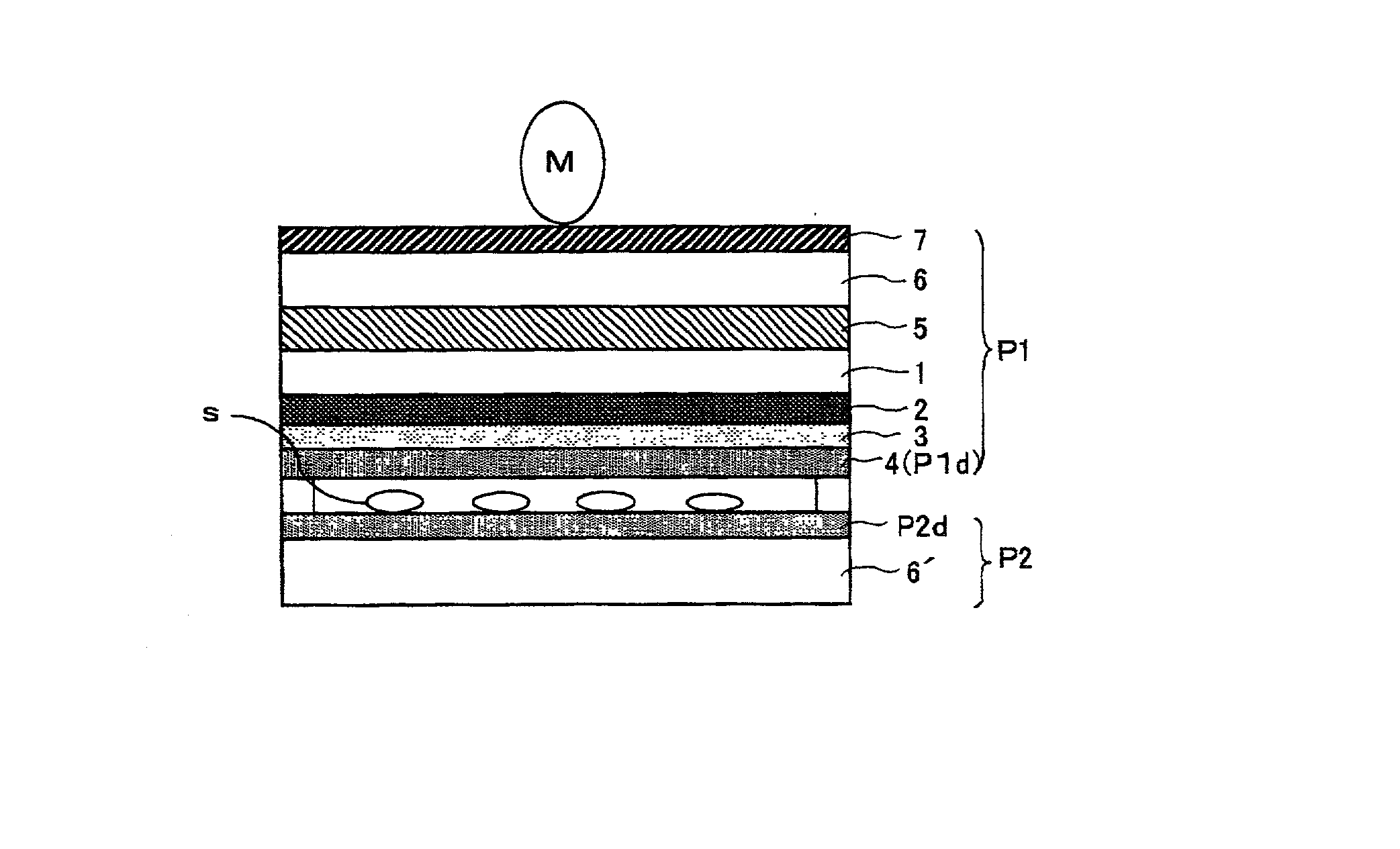
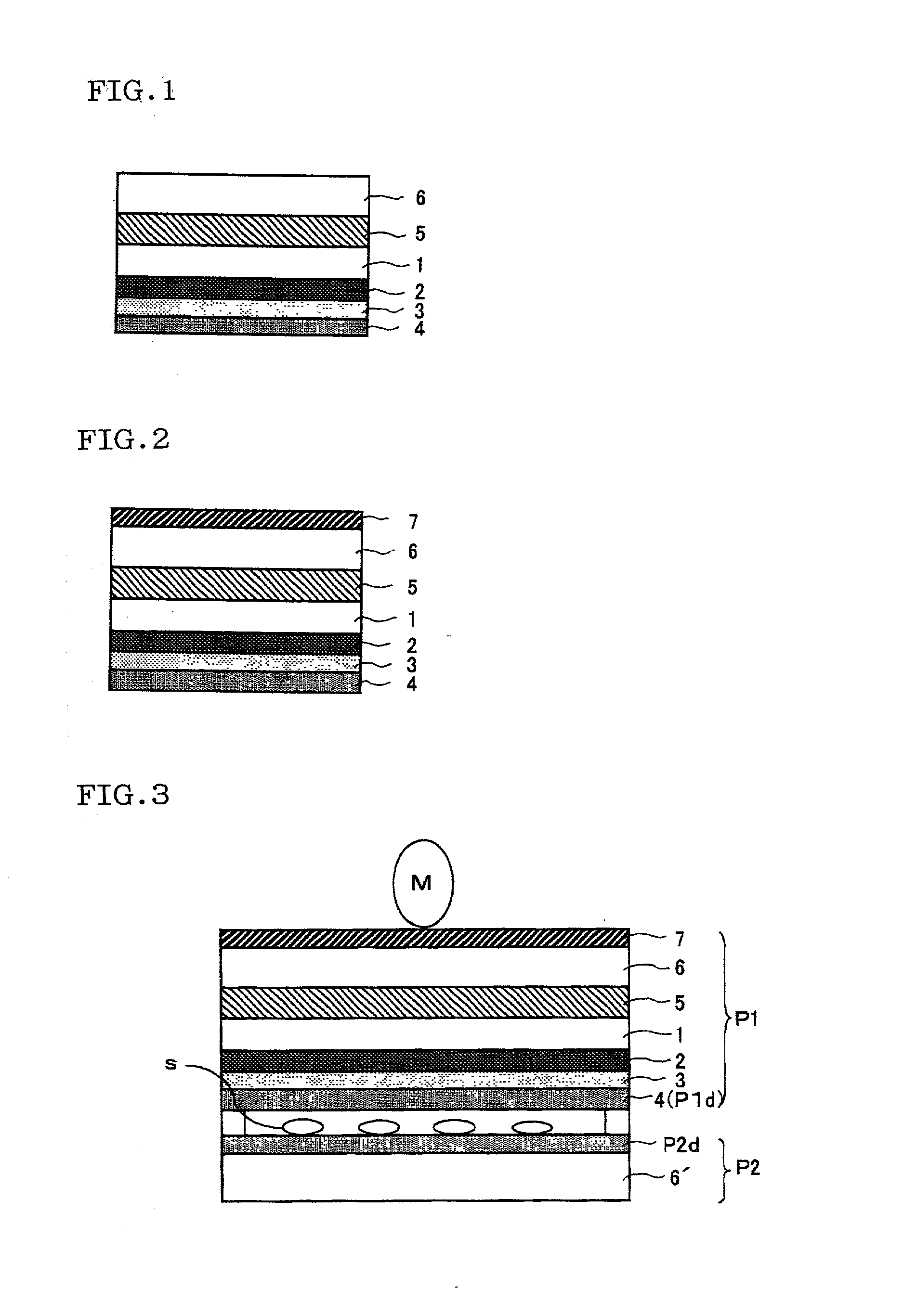
[0041] (Formation of a Dielectric Substance Thin Film)

[0042] On one face of the film substrate 1 (light index of refraction n1=1.66) comprising polyethylene terephthalate film (henceforth referred to as PET film) with a thickness of 25 .mu.m, a dielectric substance thin film 2 with a thickness of 100 nm was formed in which fine-particles of TiO.sub.2 (light index of refraction n=2.35) are mixed into a resin of thermosetting type (light index of refraction n=1.54) that comprises melamine resin:alkyd resin:organic silane condensate=2:2:1 (by weight ratio), and a composition ratio was adjusted so that it might make an index of refraction n2=1.68. Subsequently, vacuum evaporation of SiO.sub.2 (light index of refraction n3=1.46) was conducted by an electron beam heating method under a condition of 1.times.10.sup.-2 to 3.times.10.sup.-2 Pa of degree of vacuum to form a transparent dielectric substance thin film 3 (henceforth also referred to as SiO.sub.2 thin film) with about 50 nm in thi...

example 2

[0049] (Formation of a Hard Coat Processed Layer)

[0050] Hydroxy cyclohexyl phenylketone (Irgacure 184 by Ciba Specialty Chemicals K.K.) as photopolymerization initiator 5 part was added in acrylics-urethane derived resin (UNIDIC 17-806 made from DAINIPPON INK AND CHEMICALS, INCORPORATED) 100 part, and diluted to 50% by weight with toluene to obtain a toluene solution. After the toluene solution obtained above was applied to one face of a PET film whose thickness is 125 .mu.m and dryed for 3 minutes at 100 degrees C., ultraviolet rays irradiation was immediately performed using two ozone type high pressure mercury vapor lamps (80 W / cm, 15 cm condensing type), and the hard coat processed layer 7 with a thickness of 5 .mu.m was formed.

[0051] (Production of a Transparent Conductive Laminated Film, Production of a Touch Panel)

[0052] A transparent conductive laminated film of a structure shown in FIG. 2 was produced as in Example 1, except that in Example 1 the PET film with this hard coa...

example 3

[0053] In Example 1 (formation of a dielectric substance thin film), except that a thickness of the dielectric substance thin film 3 was set 2 .mu.m, a dielectric substance thin film was formed as in Example 1. Subsequent processes were performed as in Example 1, a conductive thin film was formed, and a transparent conductive laminated film was produced. Moreover, a touch panel was produced as in Example 1.


PUM

PropertyMeasurementUnit
thicknessaaaaaaaaaa
thicknessaaaaaaaaaa
thicknessaaaaaaaaaa

Abstract

A transparent conductive laminated body comprising a transparent dielectric substance thin film having two layers and furthermore a transparent conductive thin film being formed on one face of a transparent film substrate with thickness of 2 to 120 mum, and a transparent substrate being adhered on another face of the film substrate through a transparent pressure sensitive adhesive layer, wherein a relationship of n3<n1<=n2 <n4 is satisfied where a light index of refraction of the film substrate is defined as n1, a light indexes of refraction of the two layers of the dielectric substance thin films are defined as n2 and n3 from the film substrate side respectively, and a light index of refraction of the conductive thin film is defined as n4 is excellent in transparency and scratch-proof property of the conductive thin film, and, moreover, excellent also in flexibility. A touch panel using the transparent conductive laminated body concerned has an improved dotting property.

Description

[0001] 1. Field of the Invention[0002] The present invention relates to a transparent conductive laminated body, which is transparent in visible light region, having a conductive thin film on a film substrate. The transparent conductive laminated body of the present invention is used in usages of transparent electrodes for new display methods applied liquid crystal displays, and electroluminescence displays and touch panels etc. besides and antistatic and electromagnetic wave interception, etc. for transparent goods[0003] 2. Description of the Prior Art[0004] As a conventional transparent conductive thin film, a so-called conductive glass in which indium oxide thin film is formed on a glass plate is known well, but since a substrate is made of glass, the conductive glass is inferior in flexibility and workability, and it is not suitable for a certain usage. Therefore, in recent years, a transparent conductive thin film in which various kinds of plastic films including polyethylene t...

Claims


Application Information

Patent Timeline
Patent Type & Authority Applications(United States)
IPC IPC(8): G02F1/1333B32B7/02G02B6/10G06F3/041H01B5/14
CPCG02B6/10G09G2330/04G09G2300/04
Inventor SUGAWARA, HIDEONOGUCHI, TOMONORIANDOU, HIDEHIKO
Owner NITTO DENKO CORP
Why Eureka
Try Eureka