

Method and system for processing substrate
a substrate and processing method technology, applied in the direction of coatings, liquid surface applicators, electrical devices, etc., can solve the problems of low dielectric constant, easy to collapse resists, and likely to occur that cantilever adheres, and similar problems are likely to occur in the formation of porous insulating layers with low dielectric constan
- Summary
- Abstract
- Description
- Claims
- Application Information
AI Technical Summary
Benefits of technology
Problems solved by technology
Method used
Image

Examples
first embodiment
[0046] In the case of independently performing the wet processing and the supercritical drying process in the wet processing apparatus 1 and the drying apparatus 2, respectively, there is the likelihood that a wafer 9 is air-dried during transfer of the wafer 9 after the wet processing. Specifically, when the wafer 9 is air-dried on the way of transfer, a capillary force is acted on the microstructure on the wafer 9, thereby collapsing a part of the microstructure. This ruins the effect of the supercritical drying. According to the substrate processing system of the first embodiment, however, since the wafer transferring apparatus 3 is arranged between the wet processing apparatus 1 and the drying apparatus 2, a wafer 9 can be transferred from the wet processing apparatus 1 to the drying apparatus 2 in a shorter time. Further, the wafer 9 is taken out of the wet processing apparatus 1 and is transferred in the non-dried state to the drying apparatus 2 immediately after the wet proce...
second embodiment
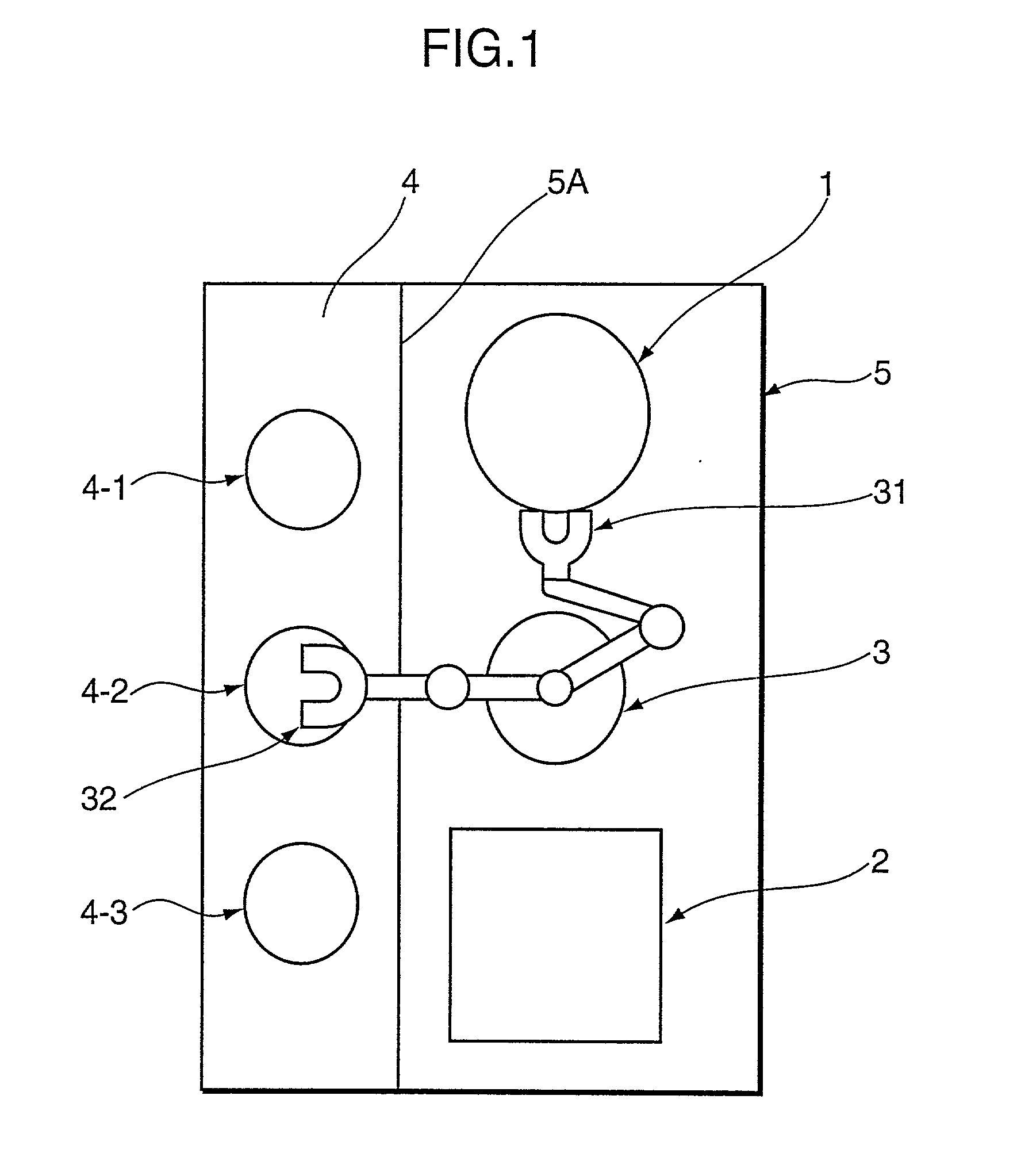
[0052] Although not illustrated, a first arm 31 and a second arm 32 of the wafer transferring apparatus 3 each have a wafer support portion and a vessel holding portion. With this arrangement, the wafer transferring apparatus 3 can transfer the transferable vessel 6 along with a wafer 9 accommodated therein. Specifically, in the second embodiment, the wafer transferring apparatus 3 and the wafer loading apparatus 7 constitute a wafer transfer.
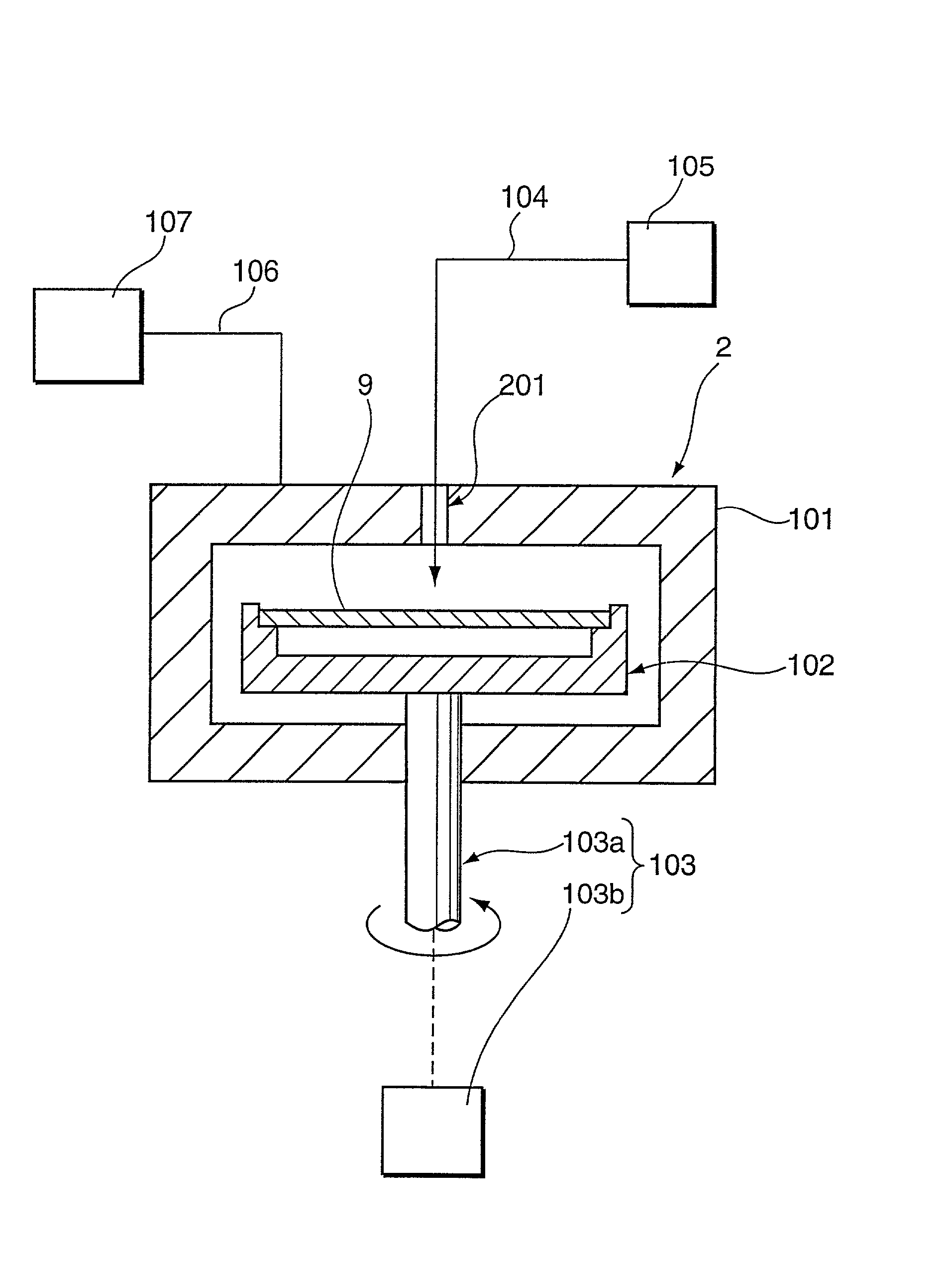
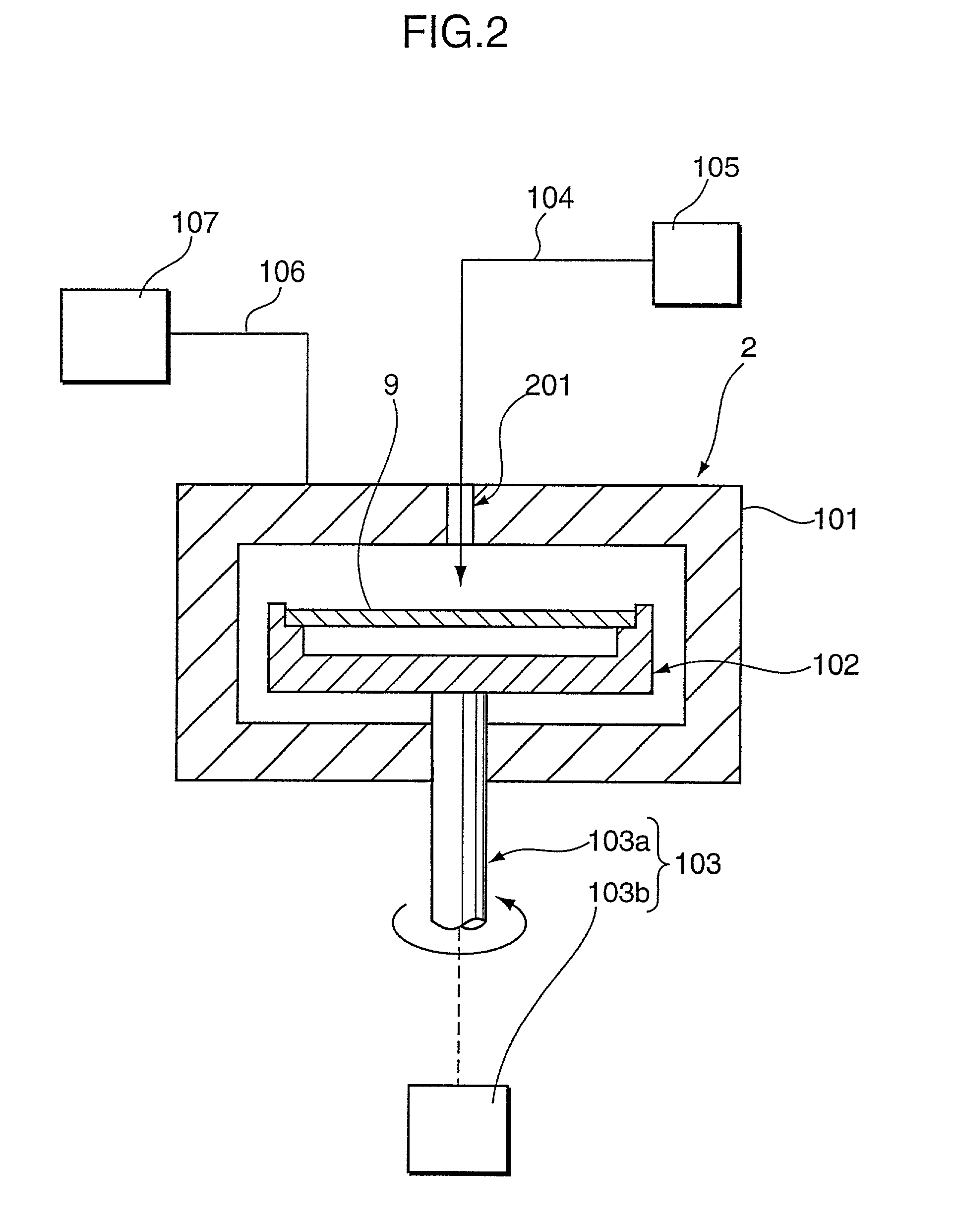
[0053] In the second embodiment, a high-pressure vessel 101 of the drying apparatus 2 is not provided with the wafer holder 102 that is provided in the first embodiment, and the transferable vessel 6 is directly linked to a rotation driving mechanism 103 of the drying apparatus 2. Further, in the second embodiment, the high-pressure vessel 101 is not provided with a liquid inlet 201 for supplying a protecting liquid (deionized water) into the high-pressure vessel 101, the supplying pipe 104, and the supplying source 105 that are provided in the...
PUM
| Property | Measurement | Unit |
|---|---|---|
| size | aaaaa | aaaaa |
| size | aaaaa | aaaaa |
| size | aaaaa | aaaaa |
Abstract
Description
Claims
Application Information