Semiconductor device

a technology of semiconductor devices and logic circuits, applied in semiconductor devices, semiconductor/solid-state device details, electrical apparatus, etc., can solve the problems of increasing power consumption, unable to meet the requirements of high-integrated logic circuits, and no longer expectable device operation speed,

Inactive Publication Date: 2002-11-07
KK TOSHIBA
View PDF0 Cites 19 Cited by
  • Summary
  • Abstract
  • Description
  • Claims
  • Application Information

AI Technical Summary

Problems solved by technology

Thus, device operation speed will no longer be expectable even when semiconductor elements such as transistors are designed to offer enhanced speed performances.
The approach is not suitable for highly integrated logic circuits.
So even with the above-noted multilayer wiring structure, it can increase in power consumption required fo...

Method used


Image

  • Semiconductor device
  • Semiconductor device
  • Semiconductor device

Examples


first embodiment

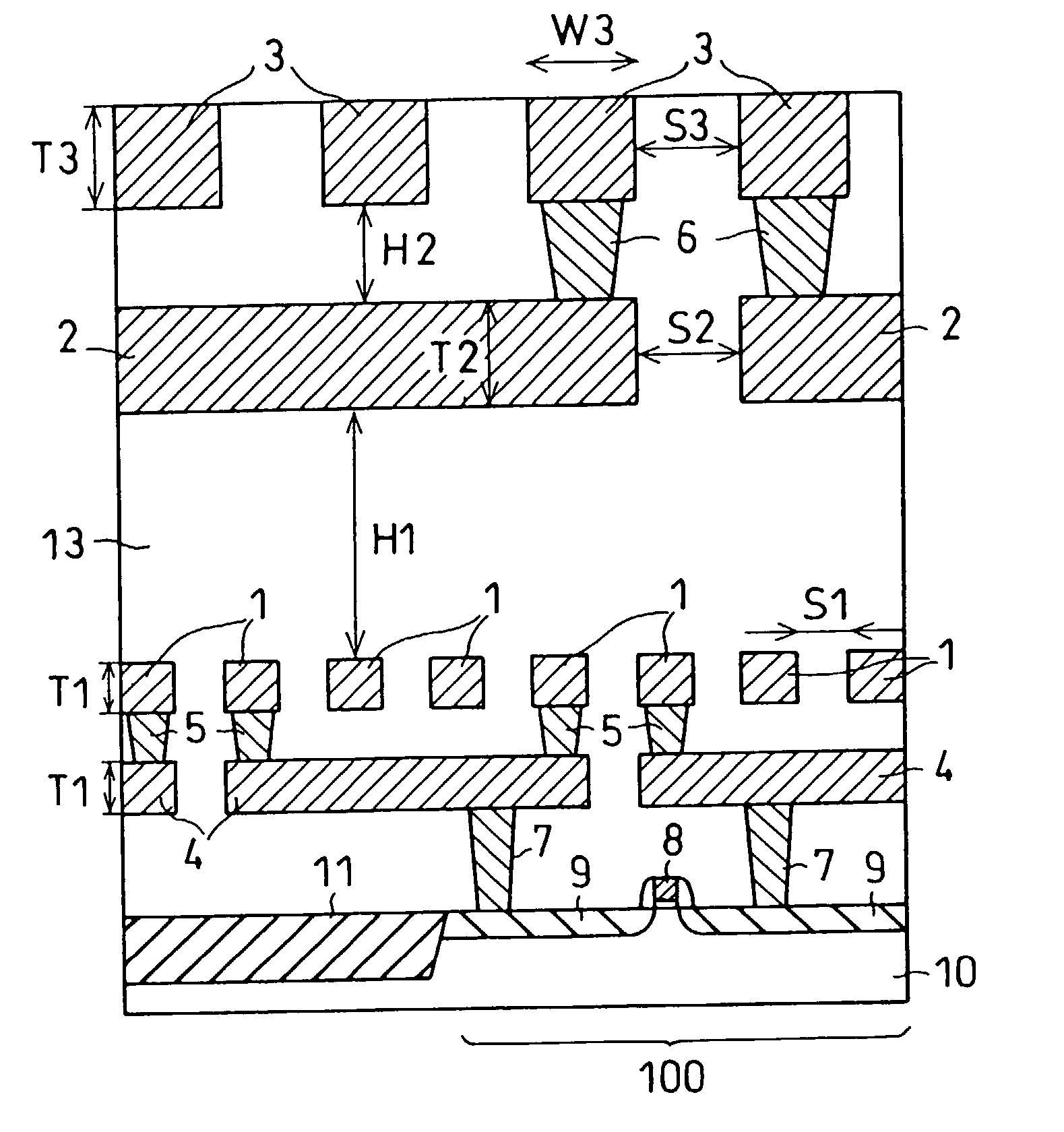
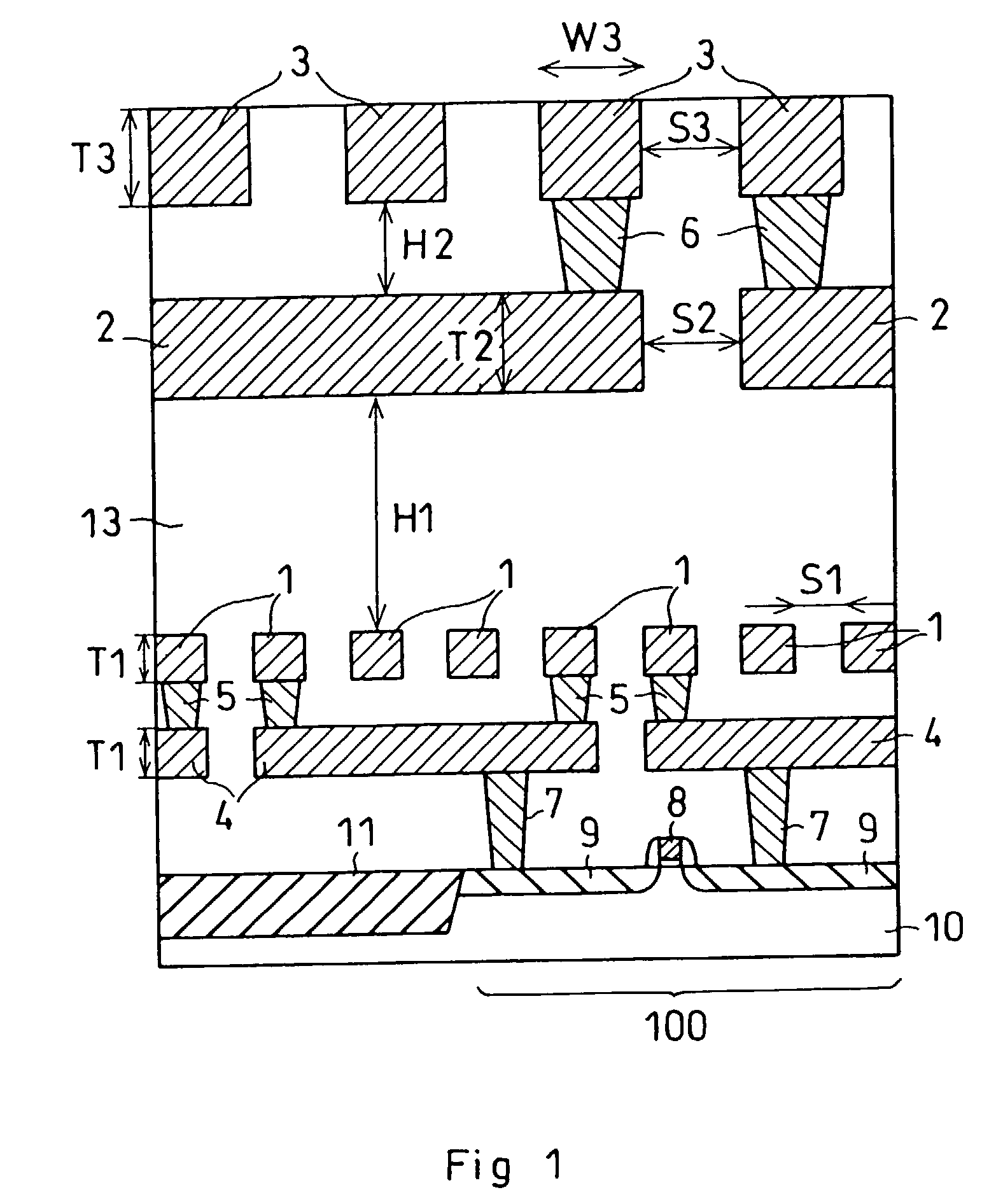
[0078] FIG. 1 is a diagram illustrating, in cross-section, a semiconductor device in accordance with the present invention. In FIG. 4, an exploded perspective view of an internal structure of the device shown in FIG. 1, including planar layout patterns of respective wirings stacked or laminated over one another. In FIG. 4, for the purpose of visually emphasizing the wirings of interest, depiction of a semiconductor substrate region and contacts is eliminated, and dotted lines indicate the connection relationship between such contacts and interconnect wirings.

embodiment 1

[0079] In the embodiment 1, the wirings are divided into two groups: "local" wirings (wiring 4 and first wiring 1), and "global" wirings (second wiring 2 and third wiring 3) as formed over the local wirings. A distance between global wiring (the second wiring 2) and local wiring (the first wiring 1) is designed to be wider than a distance between the global wirings (the second wiring 2 and the third wiring 3). A wiring thickness of global wiring (the second wiring 2 and the third wiring 3) is greater than a wiring thickness of local wiring layer (the wiring 4 and the first wiring 1). An amplitude of a signal voltage of the global wirings (the second wiring 2 and the third wiring 3) is lower than an amplitude of a signal voltage of the local wirings (the wiring 4 and the first wiring 1).

[0080] In this invention, "an amplitude of a signal voltage" of wirings means the voltage difference between two voltages that correspond to two logical states at steady states, respectively. For exam...

embodiment 2

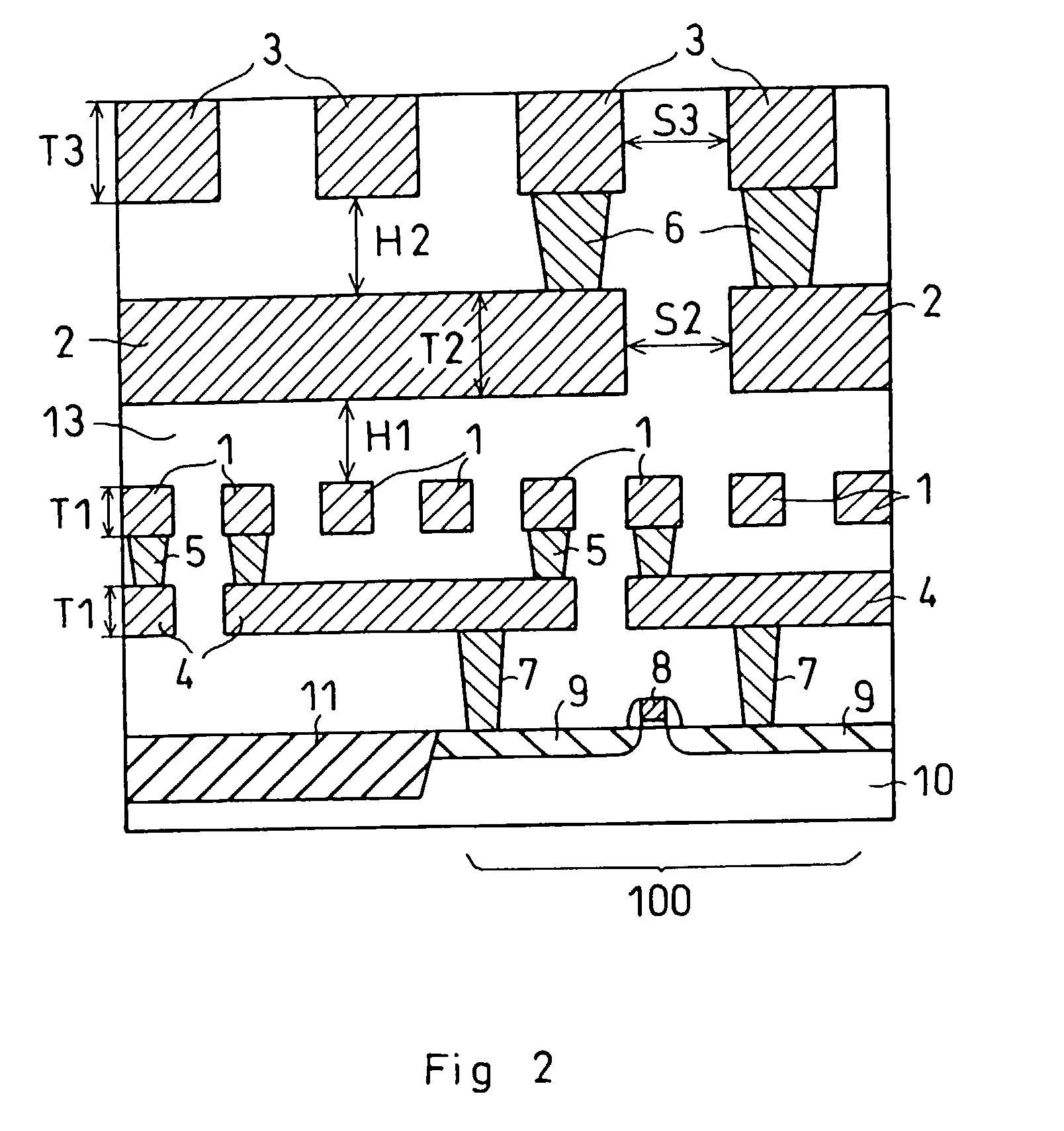
[0168] FIG. 15 is a diagram showing in cross-section a multilayer wiring structure of a semiconductor device in accordance with a second embodiment of the present invention, including a semiconductor substrate region thereof. The same parts or components as those in FIG. 1 are designated by the same reference characters, and an explanation thereof will be eliminated herein.

[0169] This embodiment shown is the one that a fourth wiring 12 is further formed over the third wiring 3 in the first embodiment stated supra, wherein a distance H1 between the first wiring 1 and the second wiring layer 2 is greater than a distance H2 between the third wiring 3 and the fourth wiring 12.

[0170] In FIG. 15, depiction of the part underlying the second wiring 2 is omitted, as it is the same in structure as that of the first embodiment set forth previously.

[0171] A insulating film 13 (a firth insulating film) is deposited on an entire upper surface of the second wiring 2 to have a thickness greater in ...


PUM


Abstract

An electrical wiring structure capable of improving a wiring delay to thereby achieve both low power consumption and high-speed performances without accompanying any significant changes in circuit layout and wiring structure of prior known CMOS logic circuitry and also alterations of the multilayer configuration of wiring layers is provided. A local wiring 1 and global wirings 2, 3 are stacked over a semiconductor substrate 10 in this order of sequence when looked at from lower part in a lamination direction, with dielectric layers sandwiched between adjacent ones of these layers. A distance between the local wiring 1 and the global wiring 2 is so formed as to be greater than a distance between the global wiring layer 2 and the global wiring, 3. Thus provided is a semiconductor device featured in that a drive voltage used to drive the global wirings 2, 3 is potentially lower than a drive voltage for driving inside of the local wiring 1.

Description

[0001] 1. Field of the Invention[0002] The present invention relates generally to semiconductor devices and more particularly to semiconductor logic circuitry having a multilayer wiring structure offering high-speed performances while reducing electrical power consumed therein.[0003] 2. Description of the Related Art[0004] Very-large-scale or ultralarge-scale semiconductor logic circuits formed of complementary metal oxide semiconductor (CMOS) transistors are such that semiconductor elements are becoming smaller in size or "shrinking" in minimum feature length. On the contrary, chip sizes are increasing year by year, so electrical interconnect wirings are longer.[0005] As the wirings are longer, electrical resistivity and / or coupling capacitances of the wirings larger than channel resistivities and diffusion layer capacitances of those transistors used to drive the wirings. Thus, device operation speed will no longer be expectable even when semiconductor elements such as transistors...

Claims


Application Information

Patent Timeline
IPC IPC(8): H01L23/522
CPCH01L23/5222H01L2924/0002H01L2924/00
Inventor NOGUCHI, MITSUHIRONISHIYAMA, AKIRA
Owner KK TOSHIBA
Why Eureka
Try Eureka