Programmable logarithmic gain adjustment for open-loop amplifiers

a technology of logarithmic gain adjustment and open-loop amplifier, which is applied in the direction of volume compression/expansion, instruments, computation using denominational number representation, etc., can solve the problems of high cost of process, precision resistor, slow amplifier performance, etc., and achieve the effect of decreasing or increasing the input resistan

Inactive Publication Date: 2002-11-28
INFINEON TECH AG
View PDF0 Cites 18 Cited by
  • Summary
  • Abstract
  • Description
  • Claims
  • Application Information

AI Technical Summary

Benefits of technology

0005] In order to address the deficiencies of the prior art, a better programmable amplifier is disclosed that meets these needs by obeying a logarithmic gain-code to gain transfer function. One embodiment of the invention is a programmable open loop amplifier having a resistance network. The resistance network has two or more resistors, connected in series, and at least one MOS transistor connected in parallel with the resistors. Each MOS transistor also has a pair of matching resistors connected in series, one on each side of the transistor, such that each series of resistor-transistor-resistor is connected in parallel with the two series resistors. The programmable controller applies either a gate voltage or ground to each transistor gate, thus setting the input resistance. The gain of the amplifier is determined by the resistance of the resistance network, in combination with the other characteristics of the amplifier circuit.
0006] Another embodiment of the invention is a programmable open loop amplifier having an input resistance network. The amplifier is open-loop because there is no direct feedback and control of the amplification or gain of the amplifier. The circuit depends on matching resistances and switching in and out of resistance branches. The resistance network includes two input resistors connected in series, and at least one pair of input MOS transistors also connected in series, each pair then connected in parallel with the other pairs and with the two series resistors. A programmable controller applies a gate voltage or ground to the gates of the transistors to turn each pair on or off, closing or opening a path between the input terminals, and decreasing or increasing the input resistance. The voltage applied to the transistors causes them to operate in a linear or triode region of their operating range. The closed switch resistance of each pair of MOS transistors is equal to a resistance of the pair of input resistors.
0007] In another embodiment of the invention, a programmable open loop amplifier has an output resistance network. The output resistance network comprises at least one pair of MOS transistors in series, with each pair connected in parallel. An output resistor connects each side of the MOS pairs to ground. The programmable controller applies a gate voltage or ground to each pair of output MOS transistors, and the gate voltage causes the transistors to operate in a linear or triode region of their operating range. Embodiments of the present invention are suitable for amplification of signals from DC to about 1GHz.

Problems solved by technology

This requires matching of precision resistors, a costly process.
In addition, using a series of resistors can add significantly to the parasitic capacitance of the input network, slowing performance of the amplifier.
This technique, however, can only be implemented with bipolar junction technologies, which are much less attractive when compared to MOS (metal-oxide semiconductor) and CMOS (complementary metal-oxide semiconductor) manufacturing techniques.
However, MOS transistors used for their resistance by biasing at very low voltages introduce distortion, increasing the total harmonic distortion of the amplifier circuit.
This is not desirable in a data acquisition system.
Finally, resistance networks of this type may require a large footprint in the circuit.
Depending on how many amplifiers are in the circuit, the penalty in both capacitance and silicon area may be great.

Method used


Image

  • Programmable logarithmic gain adjustment for open-loop amplifiers
  • Programmable logarithmic gain adjustment for open-loop amplifiers
  • Programmable logarithmic gain adjustment for open-loop amplifiers

Examples


Embodiment Construction

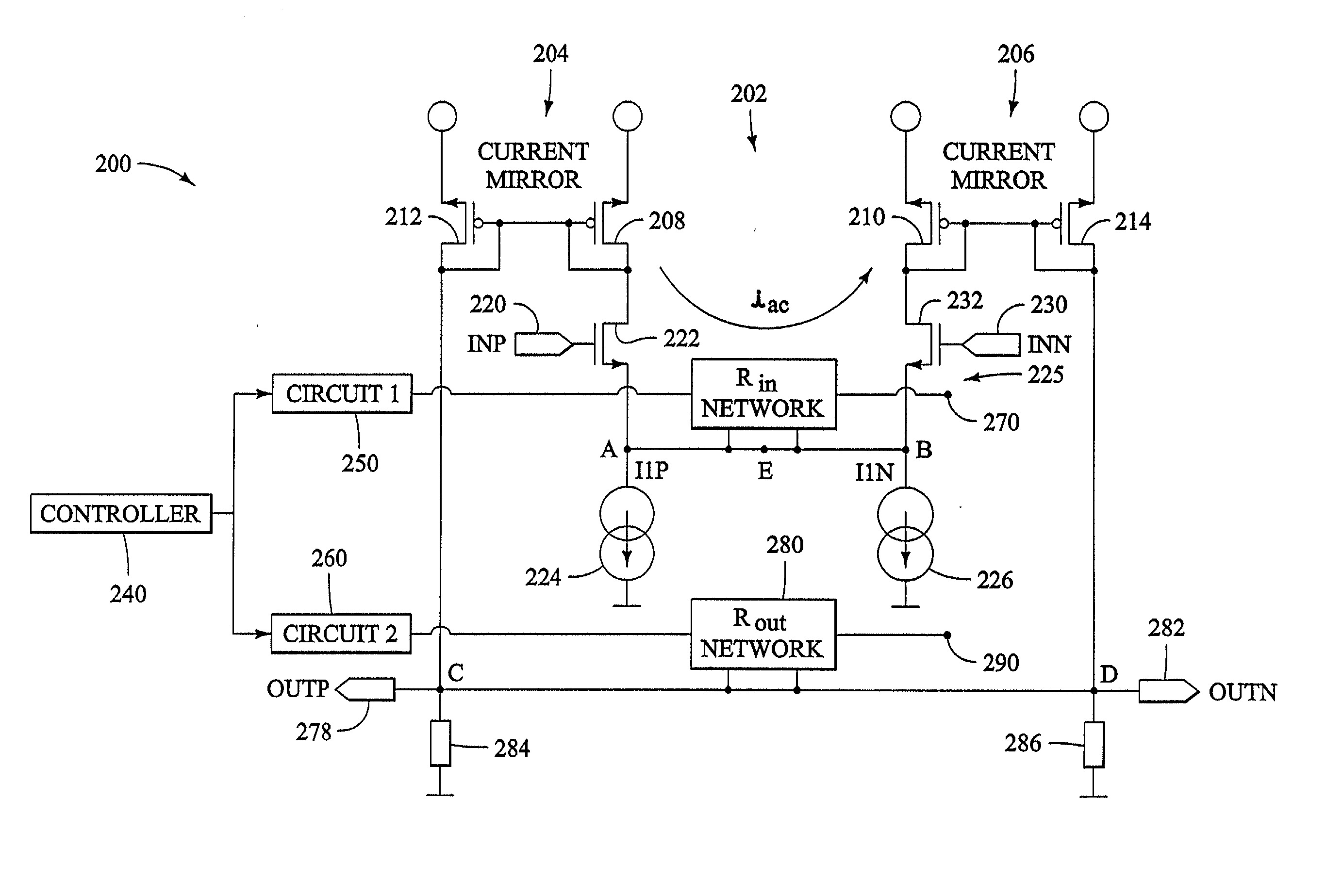
[0016] In the discussion below, transistors are described as CMOS transistors, and in particular as PMOS (positive MOS) or NMOS (negative MOS) transistors. Those skilled in the art will recognize that the terms p-channel and n-channel might more accurately describe the transistors discussed herein, since these transistors are no longer manufactured by depositing metallic elements, except possibly for external connections. Rather, polysilicon is doped to either p-channel or n-channel, indicating whether the channel between source and drain conducts via depletion mode (holes) or enhancement mode (electrons). Nevertheless, the terms PMOS and NMOS are more-commonly used, and are so used herein to mean those transistors manufactured by CMOS processes.

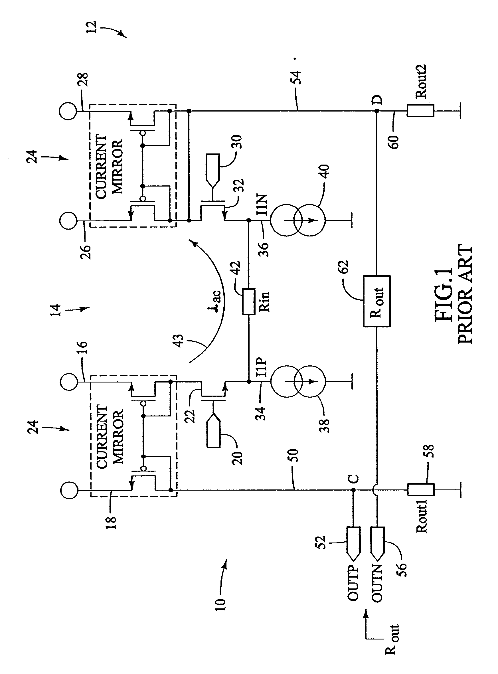
[0017] FIG. 1 is a simplified drawing of a prior art amplifier using a differential transconductance in its input and output portions. Amplifier 10 has an input portion 14 and output portions 24. The sources of transistors 16, 18, 26 and 28 ...


PUM


Abstract

Transconductance-based variable gain amplifiers amplify an input voltage by converting the voltage difference to a current and then amplifying the result. At least one resistor network is adjusted depending on the magnitude of the input voltage difference and the output desired. A network of MOS transistor switches with a small footprint adjusts the resistance of the input voltage circuit in a way to insure consistent resistance and low stray capacitance.

Description

[0001] Amplifiers having a variable gain typically adjust the gain by switching resistors in and out of their circuits. These resistances change the conductance or transconductance characteristics of the amplifier. In this manner, an amplifier can be useful over a very wide range of input signals, and in particular over decades of logarithmic variation. The performance of such amplifiers may be modeled as a product of their transconductance multiplied by a transfer function of the amplifier.[0002] Data acquisition systems may use programmable gain amplifiers in order to capture a wide variety of signals or signal amplitudes. Some programmable gain amplifiers have a gain-code to gain transfer function that is logarithmic rather than linear, which can accommodate a wide range of input signals. These amplifiers change their transconductance and thus performance by switching resistors in and out of the input network. This requires matching of precision resistors, a costly process. In ad...

Claims


Application Information

Patent Timeline
Patent Type & Authority Applications(United States)
IPC IPC(8): H03G1/00H03G7/00
CPCH03F3/45197H03G7/00H03G1/0088
Inventor CYRUSIAN, SASANBLON, THOMAS
Owner INFINEON TECH AG
Why Eureka
Try Eureka