Semiconductor memory device

a memory device and semiconductor technology, applied in the field of semiconductor memory devices, can solve the problems of psrams being used with the lack of address multiplexing, srams suffering from difficulties in achieving small size and large storage capacity, and becoming more difficult for memory cells of such semiconductor memories

Inactive Publication Date: 2002-12-05
KK TOSHIBA
View PDF7 Cites 68 Cited by
  • Summary
  • Abstract
  • Description
  • Claims
  • Application Information

AI Technical Summary

Problems solved by technology

As semiconductor memory devices decrease in size and power dissipation while increasing in storage capacity, it is becoming more difficult for memory cells of such semiconductor memories, in particular those having ultrafine or "micro" structures, to attain high reliability in view of fabrication process technologies and also transistor characteristics.
Due to the use of multiple transistors per cell, SRAMS suffer from difficulties in achievement of small size and large storage capacity.
Accordingly, direct use of SRAM interface would result in PSRAMs being used with the lack of any address multiplexing.
It is apparent from the foregoing discussion that the use of PSRAMs enables achievement of smaller system sizes and thus larger storage capacities (higher integration densities), although this approach accompanies a penalty that PSRAMs become greater in data retain currents than SRAMs due to employment of DRAM-based cell designs.
Unfortunately, in cases where an attempt is made to achieve further reduced power consumption, the resultant memory cells decrease in data retaining characteristics.
The degradation of data storing performance causes a problem as to unwanted generation of defective data even when PSRAMs are designed to come with on-chip automatic refresh circuitry.
It can cause problems in standard DRAMs and also in electrically erasable and programmable read-only memory (EEPROM) chips.

Method used


Image

  • Semiconductor memory device
  • Semiconductor memory device
  • Semiconductor memory device

Examples


case 7 -

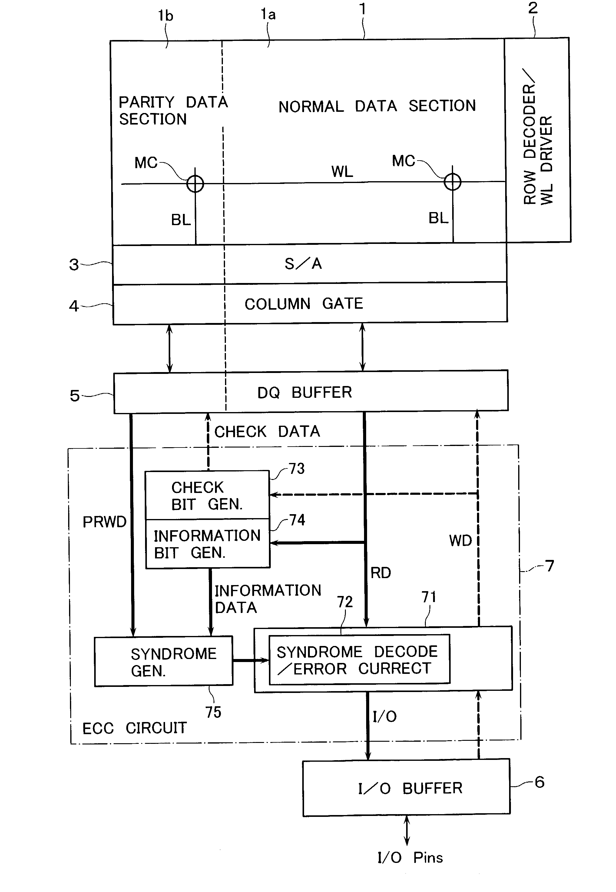
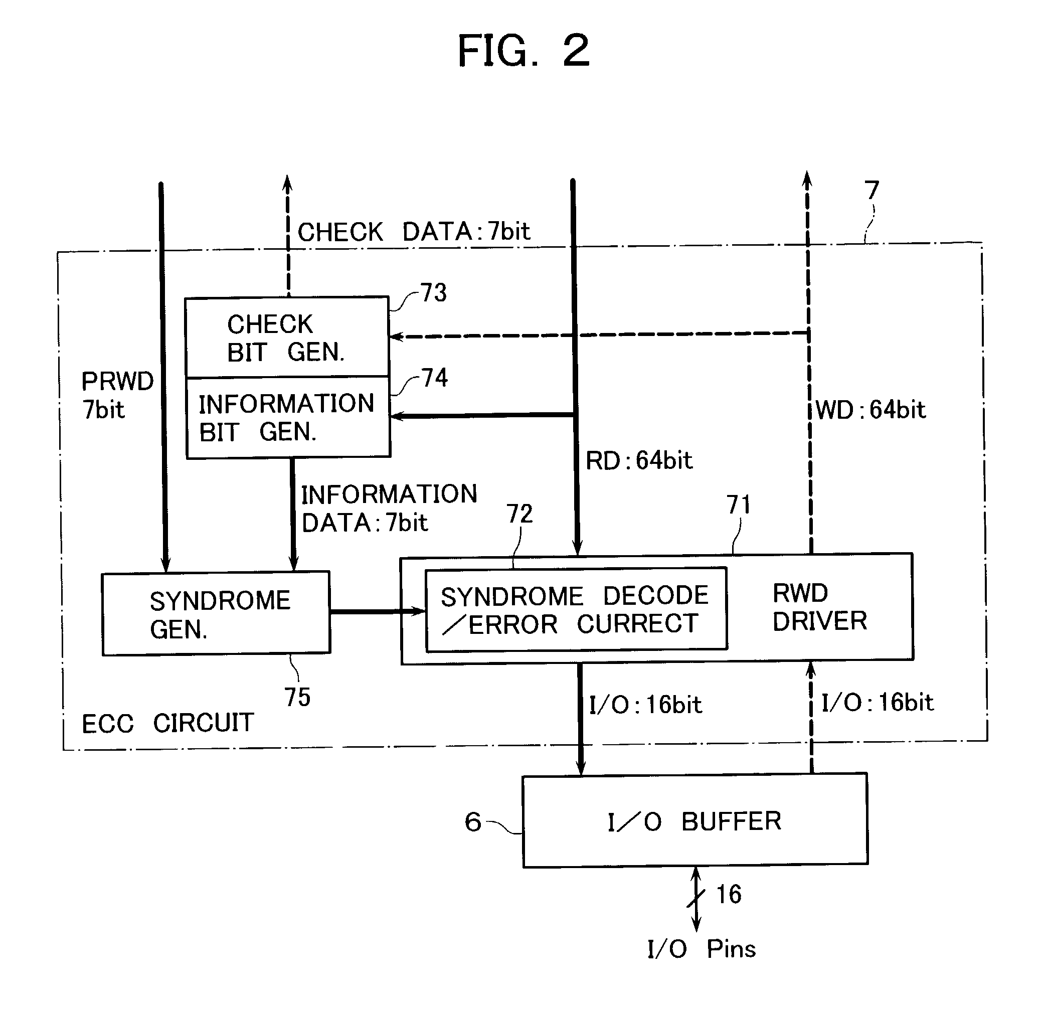
[0047] In case 7-bit check data is used as in the FIG. 2 embodiment, the Hamming-code check matrix and code are given as 7-digit binary numbers other than zero (0). At this time, while the syndrome signal is for obtaining a 1-bit error address of the check matrix, the syndrome decode circuit is preferably arranged to have a NOR / NAND configuration as shown in FIG. 7. This circuit configuration is preferable in view of the fact which follows: upon occurrence of errors of more than 2 bits, a 7-bit syndrome with all bits of "1"s can sometimes be generated; at this time, the use of circuitry for detecting and decoding only "1"s or "0"s of the syndrome would result in a plurality of inherently right data items being rewritten unintentionally.

[0048] More specifically the syndrome decoder is arranged including a parallel combination of a 3-input NAND gate G1 for detecting that all of the "1" data bits of a 7-digit syndrome signal are "1" and a 4-input NOR gate G2 for detecting that its "0" ...


PUM


Abstract

A semiconductor memory device is disclosed which comprises a cell array including a normal data section used for normal data write and read and a parity data section used for check data write and read, the check data being for execution of error check of data as read out of the normal data section, a data buffer for temporal stage of read data from the cell array and write data into the cell array, and an ECC circuit for generating the check data to be stored in the parity data section from write data as input during data writing, and for performing error check and correction of data read out of the normal section based on the data read out of the normal data section and the check data read out of said parity data section during data reading. N-bit parallel data transfer is performed between the data buffer and normal data section whereas m-bit parallel data transfer is done between the data buffer and external input/output terminals (where m and n are integers satisfying m<n).

Description

[0001] This application is based on and claims the benefit of priority from prior Japanese Patent Application No. 2001-168706, filed on Jun. 4, 2001, the entire content of which is incorporated herein by reference.[0002] 1. Field of the Invention[0003] This invention relates generally to semiconductor memory devices and more particularly to a semiconductor memory device capable of recovering or "rescuing" data defects occurring due to the quest for lower electrical power consumption.[0004] 2. Description of the Related Art[0005] As semiconductor memory devices decrease in size and power dissipation while increasing in storage capacity, it is becoming more difficult for memory cells of such semiconductor memories, in particular those having ultrafine or "micro" structures, to attain high reliability in view of fabrication process technologies and also transistor characteristics. Semiconductor memories include static random access memory (SRAM) chips with an array of memory cells, eac...

Claims


Application Information

Patent Timeline
Patent Type & Authority Applications(United States)
IPC IPC(8): G06F11/10G11C7/24G11C11/4078
CPCG06F11/1032G11C11/4078G11C7/24
Inventor KOGA, MITSUHIROYOSHIDA, MUNEHIROSHINYA, HIROSHI
Owner KK TOSHIBA
Why Eureka
Try Eureka