
Semiconductor device having an ESD protective circuit

Inactive Publication Date: 2002-12-26
RENESAS ELECTRONICS CORP
View PDF0 Cites 22 Cited by
  • Summary
  • Abstract
  • Description
  • Claims
  • Application Information

AI Technical Summary

Benefits of technology

[0027] In accordance with the semiconductor device of the present invention, the floating gate MOSFET first operates in a pinch-off mode due to the potential rise of the control gate receiving an excessively high input voltage, thereby generating positive holes in the semiconductor substrate. The positive holes thus generated trigger the floating gate MOSFET to operate in a uniform bipolar mode due to the presence of a parasitic bipolar transistor in the floating gate MOSFET. The uniform bipolar mode operation of the floating gate MOSFET allows a uniform snapback breakdown thereof, whereby the protective circuit can protect the internal circuit against the excessively high input voltage which may have a relatively lower voltage compared to a clock signal, for example, without causing a damage of the protective device itself.

Problems solved by technology

It is known that MOSFETs are liable to ESD breakdown wherein an excessively high input voltage such as an electrostatic pulse voltage enters and damages the semiconductor device.
This leads to increase in the probability of the ESD breakdown of the semiconductor elements, especially of the MOSFETs, having smaller dimensions and packed with a higher density.
Thus, the local area at which the avalanche breakdown first occurred is likely to be damaged by the ESD breakdown.
In addition, the nMOSFET is liable to damages by a breakdown in the gate insulation film thereof.
In the conventional protective circuit of FIG. 2, if a high input voltage which does not cause the avalanche breakdown is applied to the input terminal, the protective circuit cannot respond to the high input voltage.
Since the avalanche breakdown voltage cannot be adjusted to a satisfactory lower level, it is difficult to obtain a protective circuit of FIG. 2 having a desired operational voltage.
As a common problem in the protective circuits of FIGS. 1A and 2, the MOSFETs provided in the protective circuits have larger dimensions compared to the other MOSFETs in the internal circuit.
In this configuration, the local avalanche breakdown has a tendency to activate a specific unit MOSFET among the ten unit MOSFETs, whereby the breakdown current concentrated at the single unit MOSFET damages the same and thus the protective circuit itself.
However, the protective circuit of FIG. 3 has a drawback wherein this type of nMOSFET cannot be used as an output buffer.

Method used


Image

  • Semiconductor device having an ESD protective circuit
  • Semiconductor device having an ESD protective circuit
  • Semiconductor device having an ESD protective circuit

Examples


first embodiment

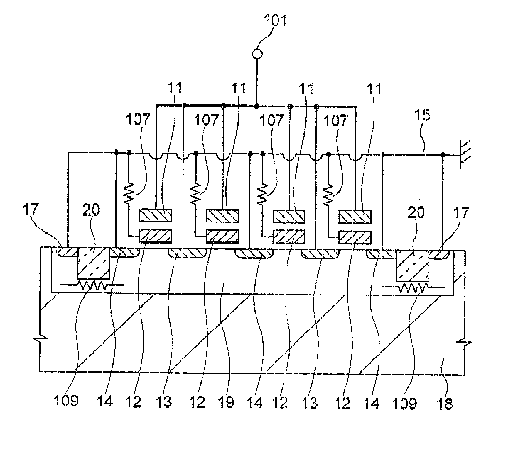
[0045] Now, the present invention is more specifically described with reference to accompanying drawings. Referring to FIG. 4, an ESD protective circuit (simply referred to as protective circuit hereinafter) according to the present invention includes a floating gate nMOSFET 104 connected between an input / output line (I / O line) 102 connected to an input / output terminal (I / O terminal) 101 and ground line VSS. The I / O line 102 is connected to a gate of a MOSFET in an internal circuit via a protective resistor 103.

[0046] The nMOSFET 104 includes a control gate 105 connected to the I / O line 102, a floating gate 106 connected to the ground line VSS via a floating gate resistor 107, and a backgate 108 connected to the ground line VSS via a backgate resistor 109.

[0047] Referring to FIG. 5, another protective circuit according to the first embodiment is similar to the protective circuit of FIG. 4, except that a floating gate nMOSFET 104a is connected between the I / O line 102 and the ground ...

second embodiment

[0065] Referring to FIG. 9, a protective circuit according to the present invention is connected between a pair of I / O terminals 21 and 22, which are applied with different source voltages.

[0066] In FIG. 9, a first I / O line 22 is connected to the first I / O terminal 21, and connected to the internal circuit via a resistor, whereas a second I / O line 24 is connected to the second I / O terminal, and to the internal circuit via a resistor.

[0067] The protective circuit includes a first floating gate nMOSFET 25 and a second floating gate nMOSFET 26, the source / drain paths of which are connected in parallel between the first I / O line 22 and the second I / O line 24. The first floating gate nMOSFET 25 has a control gate 45 connected to the first I / O line 22, and a floating gate 46 connected to the ground line VSS via a floating gate resistor 27. The second floating gate nMOSFET 26 has a control gate 47 connected to the second I / O line 24, and a floating gate 48 connected to the ground line VSS ...

fourth embodiment

[0069] Referring to FIG. 11, the present invention is such that the present invention is applied to output buffers. More specifically, the protective circuit of the present embodiment includes a floating gate pMOSFET 36a and a floating gate nMOSFET 36 connected in series between the VCC line and the ground line VSS. An output terminal 34 is connected to an output line 35, which is connected to the node connecting the gloating gate pMOSFET 36a and the floating gate nMOSFET 36.

[0070] The control gates 37a and 37 of both the floating gate pMOSFET 36a and the floating gate nMOSFET 36 are connected together and also to the output line 35. The floating gates 38a and 38 of both the floating gate pMOSFET 36a and the floating gate nMOSFET 36 are connected together of an output signal line 39 from the internal circuit. The backgate 41a of the floating gate pMOSFET 36a is connected to the VCC line via floating gate resistor 42a, whereas the backgate 41 of the floating gate nMOSFET 36 is connec...


PUM


Abstract

A protective circuit includes a floating gate MOSFET having a source-drain path connected between an I / O line and a source line or a ground line, a control gate connected to the I / O line and a floating gate connected to the source line or the ground line.

Description

[0001] (a) Field of the Invention[0002] The present invention relates of a semiconductor device having an ESD (electrostatic-discharge) protective circuit and, more particularly, to a semiconductor device having an ESD protective circuit for protecting the internal circuit of the semiconductor device against the ESD breakdown.[0003] (b) Description of the Related Art[0004] A semiconductor integrated circuit (or semiconductor device) fabricated on a semiconductor substrate generally includes semiconductor elements such as MOSFETs. It is known that MOSFETs are liable to ESD breakdown wherein an excessively high input voltage such as an electrostatic pulse voltage enters and damages the semiconductor device. Thus, a technique for protecting the semiconductor elements in the semiconductor device against the damage caused by and ESD breakdown is essential to the semiconductor device. A large number of proposals have been made and used heretofore for the technique.[0005] Along with the hi...

Claims


Application Information

Patent Timeline
IPC IPC(8): H01L21/336H01L21/822H01L21/8247H01L21/8238H01L23/60H01L23/62H01L27/02H01L27/04H01L27/06H01L27/088H01L27/092H01L27/115H01L29/78H01L29/788H01L29/792H02H3/22H02H7/20H03K17/08H03K19/003
CPCH01L27/0274H01L2924/0002H01L2924/00
Inventor HIRATA, MORIHISA
Owner RENESAS ELECTRONICS CORP
Learn More