

Optical waveguide module
a technology of optical waveguides and modules, applied in the direction of electrical devices, semiconductor devices, instruments, etc., can solve the problems of increasing the number of optical components, the structure and manufacturing process of the optical circuit becomes more complicated, and the optical intensity cannot be correctly monitored, so as to prevent any deterioration in long-term stability, monitor the optical intensity accurately, and simplify the structure and manufacturing process of the optical circui
- Summary
- Abstract
- Description
- Claims
- Application Information
AI Technical Summary
Benefits of technology
Problems solved by technology
Method used
Image

Examples
first embodiment
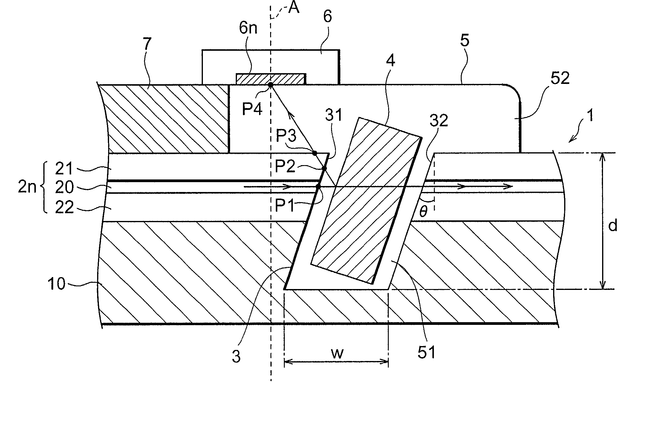
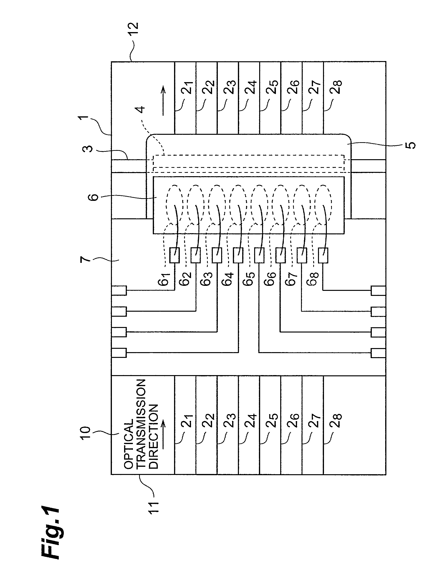
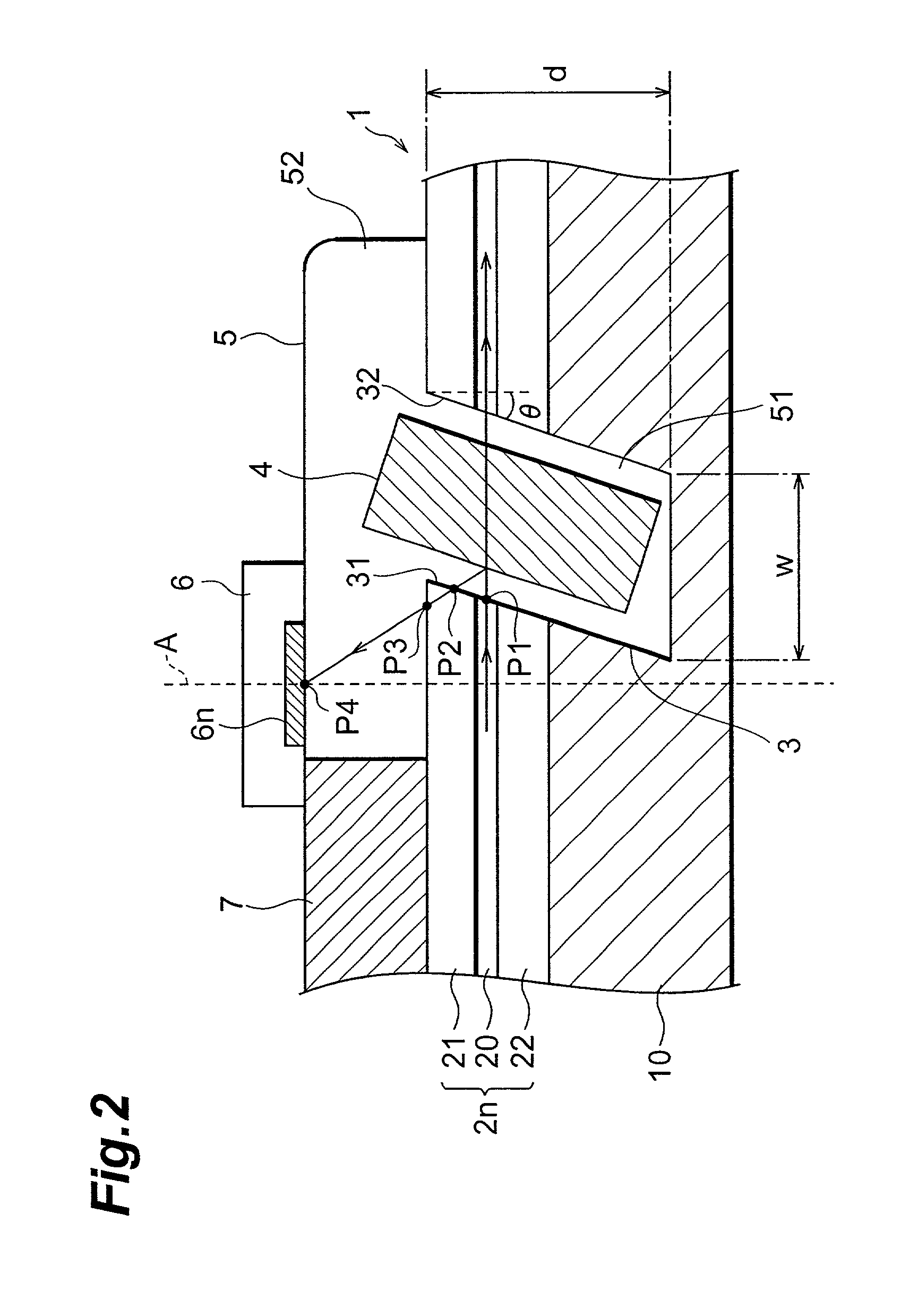
[0029] FIG. 1 is a plan view of the structure in the optical waveguide module according to the present invention. This optical waveguide module comprises a planar waveguide optical circuit 1 having a substrate 10 and eight (eight channels) planar waveguide type of optical waveguides 2.sub.1 to 2.sub.8 formed on the substrate 10.
[0030] The optical waveguides 2.sub.1 to 2.sub.8 are formed parallel to each other and equidistantly, extending from an input end 11 of the planar waveguide optical circuit 1 to an output end 12 in a predetermined optical transmission direction (the direction indicated by the arrow in FIG. 1). A groove 3 that cuts across the optical waveguides 2.sub.1 to 2.sub.8 is provided at a specific location with respect to the optical transmission direction of the planar waveguide optical circuit 1.
[0031] On the inside of this groove 3 is installed a reflection filter 4 for reflecting part of the signal light transmitted through the optical waveguides 2.sub.1 to 2.sub.8...
second embodiment
[0086] In the second embodiment, in which this problem of crosstalk between channels was handled by directly installing the photodetector array 60 on the top side of the planar waveguide optical circuit 1, without providing a sub-mounting substrate or the like, the reflected light path from the reflection filter 4 to the photodetector 61.sub.n is shorter and the spreading of reflected light can be reduced, as shown in FIG. 6. Also reduced is the effect of scattered reflection or scattering at the interface or on the inside of the optical waveguides 2.sub.n or filler resin 5. Therefore, crosstalk between the channels is suppressed.
[0087] Also, enhancing the confinement of the signal light within the core 20 with respect to the signal light transmitted through the optical waveguides 2.sub.n is preferable in terms of preventing crosstalk in both the first and second embodiments. In specific terms, the refractive index differential .DELTA.n between the core 20 and the cladding 21 and 22...
third embodiment
[0148] In this embodiment, just as the light blocking layers 25.sub.1 to 25.sub.7 in the third embodiment shown in FIGS. 7 and 8, light blocking layers 26.sub.1 to 26.sub.7 are provided to the reflected light paths from the reflection filter 4 to the photodetectors 67.sub.1 to 67.sub.8 as light path isolation means for isolating the reflected light paths from each other within the planar waveguide optical circuit 1. As mentioned above, this effectively prevents the generation of crosstalk between adjacent channels.
[0149] With this structure, in which the upper filler resin 52 is provided by filling the space between the photodetector array 66 and the upper cladding 21 of the optical waveguides 2.sub.1 to 2.sub.8 with a resin, even if bumps or the like are on the surface of the upper cladding 21, any light scattering or scattered reflection caused by these is suppressed.
[0150] As an example, in a state in which crosstalk has worsened to -20 dB, providing a light blocking layer within...
PUM
 Abstract
Description
Claims
Application Information