Oriented ferroelectric thin-film device and method for manufacturing the same

a ferroelectric thin-film device and oriented technology, applied in the direction of device material selection, coatings, chemistry apparatuses and processes, etc., can solve the problems of difficult prevention, not necessarily easy to obtain the above-mentioned oriented ferroelectric thin-film device, and high cost of providing vacuum equipment such as a deposition chamber

Inactive Publication Date: 2003-04-03
MURATA MFG CO LTD
View PDF3 Cites 12 Cited by
  • Summary
  • Abstract
  • Description
  • Claims
  • Application Information

AI Technical Summary

Problems solved by technology

However, it is not necessarily easy to obtain the above oriented ferroelectric thin-film device in which a ferroelectric oxide thin-film having excellent crystallinity and uniaxial orientation is disposed on a single crystal substrate.
However, when the single crystal substrate comprises Si or Al.sub.2O.sub.3 having a small thermal contractive force, this method is not effective because compression stress cannot sufficiently be applied to the thin-film and it is thus difficult to prevent the formation of the 90.degree. domain.
However, according to this method, there is a problem in that cost of providing vacuum equipment such as a deposition chamber is high and production cost is also high due to an increase in the number of production steps because ultra high vacuum is required to form the PbTiO.sub.3 layer.
Furthermore, the production cost is increased due to the use of expensive single crystal substrates.
Therefore, a substrate for forming the conductive thin-film thereon must be a monocrystalline oxide, which is expensive, or a layered substrate such as an Si substrate having a complicated structure.
Thus, there is a problem in that the production process is complicated and the production cost is increased.
When the thickness is less than 5 nm, the first ferroelectric sub-layer cannot provide stress to the second ferroelectric sub-layer so that the formation of a 90.degree. domain cannot be prevented.
When the thickness is more than 100 nm, the thickness is too large for practical use.
When the rate is 5 nm / minute or less, the rate is too slow for practical use.

Method used


Image

  • Oriented ferroelectric thin-film device and method for manufacturing the same
  • Oriented ferroelectric thin-film device and method for manufacturing the same
  • Oriented ferroelectric thin-film device and method for manufacturing the same

Examples


Embodiment Construction

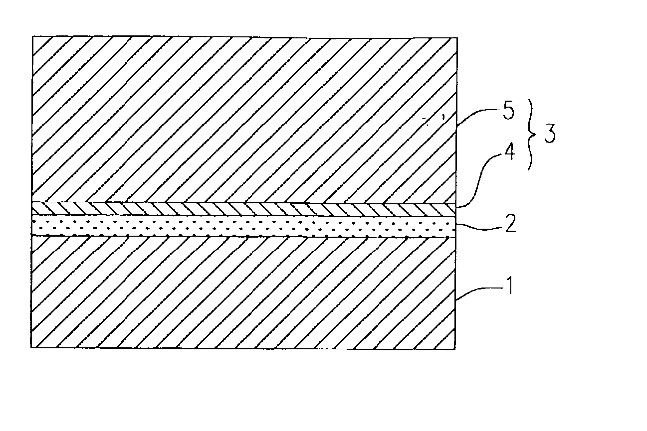
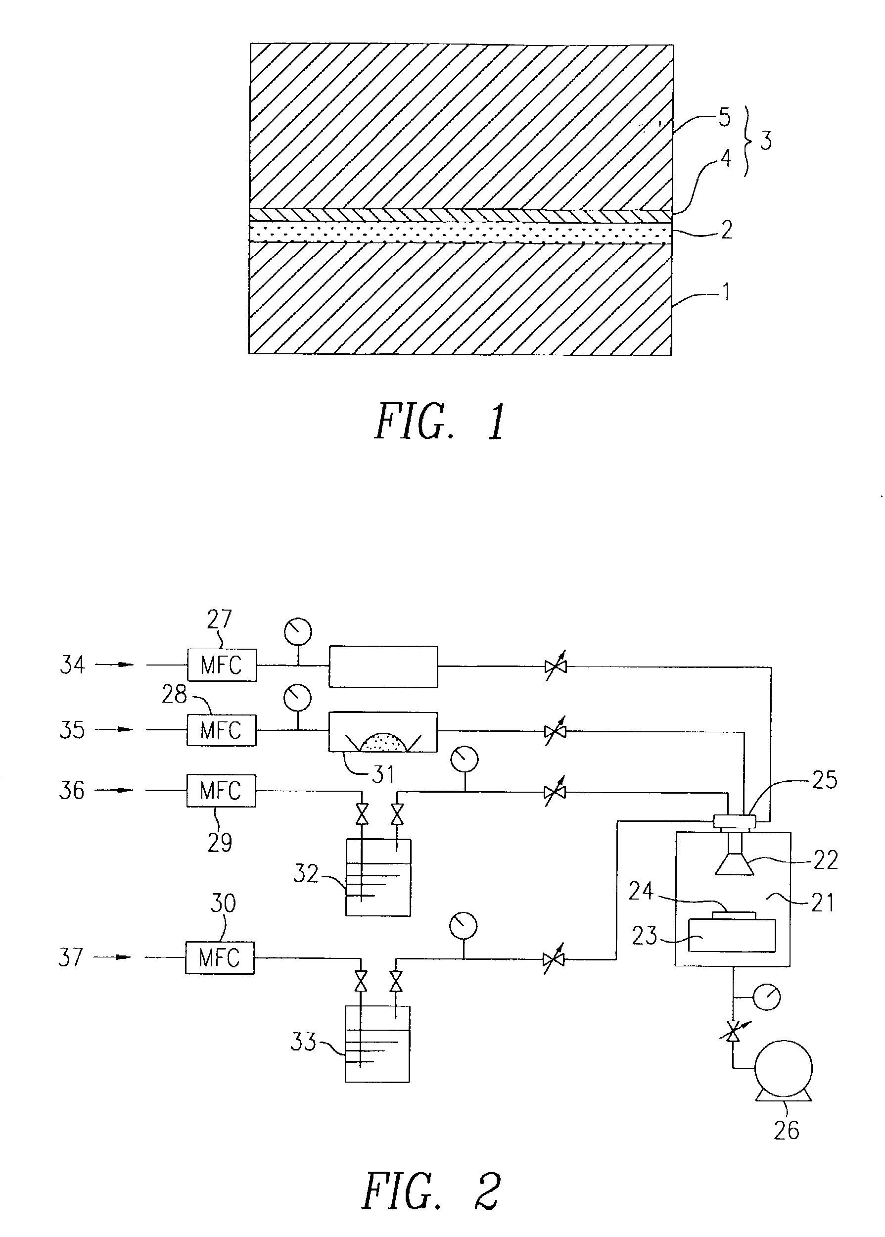
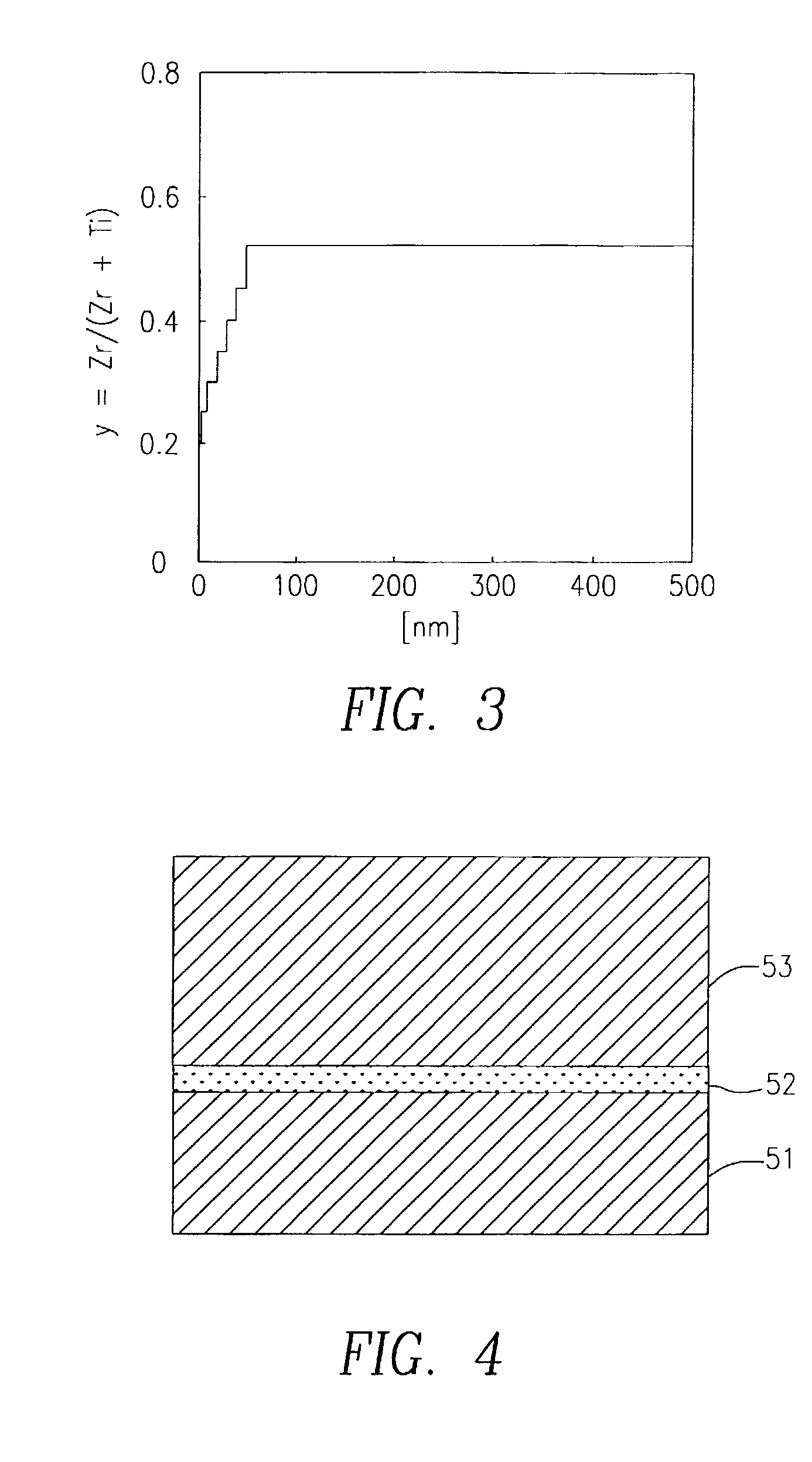
[0060] FIG. 4 is an illustration of a ferroelectric thin-film device according to a comparative example. The ferroelectric thin-film device of this comparative example includes a substrate 51, a conductive thin-film 52 disposed on the substrate 51, and a ferroelectric thin-film 53 disposed on the conductive thin-film 52, wherein the substrate 51 comprises a Si (100) single crystal, the conductive thin-film 52 comprises polycrystalline Pt--Ti, and the ferroelectric thin-film 53 comprises a Pb-containing perovskite oxide expressed by the formula Pb(Zr.sub.0 52Ti.sub.0 48)O.sub.3 and has a constant composition.

[0061] This ferroelectric thin-film device was prepared according to the following procedure.

[0062] (1) In the same way as in the above example, a Ti thin-film with a thickness of 50 nm and a Pt thin-film with a thickness of 100 nm were continuously formed on the substrate 51 comprising the Si (100) single crystal in that order by a DC magnetron sputtering process under the follo...


PUM

PropertyMeasurementUnit
thicknessaaaaaaaaaa
thicknessaaaaaaaaaa
thicknessaaaaaaaaaa

Abstract

An oriented ferroelectric thin-film device includes a substrate, a conductive thin-film disposed on the substrate, and a ferroelectric thin-film disposed on the conductive thin-film, wherein the conductive thin-film comprises a polycrystalline conductive material, the ferroelectric thin-film comprises a Pb-containing perovskite oxide and includes a first ferroelectric sub-layer and a second ferroelectric sub-layer, the first ferroelectric sub-layer is disposed on the conductive thin-film and has a composition changing in the thickness direction, and the second ferroelectric sub-layer is disposed on the first ferroelectric sub-layer and has a constant composition. The ferroelectric thin-film is oriented in a uniaxial direction such that the c-axis is perpendicular to the substrate. A method for manufacturing the oriented ferroelectric thin-film device includes the steps of forming a polycrystalline conductive thin-film on a substrate, and forming a ferroelectric thin-film on the polycrystalline conductive thin-film.

Description

[0001] 1. Field of the Invention[0002] The present invention relates to ferroelectric thin-film devices having a highly oriented ferroelectric thin-film disposed on a substrate, and particularly relates to an oriented ferroelectric thin-film device applicable to capacitors for DRAM and ferroelectric RAM, pyroelectric devices, microactuators, thin film capacitors, compact piezoelectric devices and other suitable devices. The present invention also relates to a method for manufacturing the oriented ferroelectric thin-film device.[0003] 2. Description of the Related Art[0004] Studies have recently been conducted on oriented ferroelectric thin-film devices having a ferroelectric thin-film disposed on a single crystal substrate, wherein the ferroelectric thin-film comprises a Pb-containing perovskite compound such as PZT and PLZT having large residual polarization. In the oriented ferroelectric thin-film devices, spontaneous polarization can be arranged in one direction, thereby obtainin...

Claims


Application Information

Patent Timeline
Patent Type & Authority Applications(United States)
IPC IPC(8): C23C16/18C01G25/00C23C16/40C23C16/44C23C16/455H01L21/02H01L21/314H01L21/316H01L21/8246H01L27/105H01L41/08H01L41/18H01L41/22H01L41/319
CPCC23C16/409C23C16/45523H01L21/31691H01L41/319H01L41/1876H01L41/316H01L28/56H01L21/02197H01L21/02293H10N30/8554H10N30/076H10N30/079
Inventor SAKURAI, ATSUSHIMINAMIKAWA, TADAHIRO
Owner MURATA MFG CO LTD
Why Eureka
Try Eureka