
Low dielectric constant compositions and methods of use thereof

Inactive Publication Date: 2006-05-11
RENESSELAER POLYTECHNIC INST
View PDF6 Cites 3 Cited by
  • Summary
  • Abstract
  • Description
  • Claims
  • Application Information

AI Technical Summary

Problems solved by technology

As minimum device features shrink below 0.25 microns, the increase in propagation delay, cross-talk noise and power dissipation of the interconnect structure become limiting factors.
One problem with essentially all candidates for low-k dielectrics is that copper has a relatively high diffusion coefficient in them, particularly when such dielectrics are rendered porous as a means of lowering the effective dielectric constant.
When the copper layers are contacted with the dielectric layer, the copper will diffuse into the dielectric layer under an electrical bias at an elevated temperature, and will degrade the performance of the device.
The additional layer adds to the cost of processing, occupies valuable space, and requires an even lower dielectric constant for the dielectric material that is used in conjunction with such a barrier layer in order to meet the above requirements for the effective dielectric constant of the material between the copper interconnects.

Method used


Image

  • Low dielectric constant compositions and methods of use thereof
  • Low dielectric constant compositions and methods of use thereof
  • Low dielectric constant compositions and methods of use thereof

Examples


example 1

[0056] Preparation of a Cyclolinear Unsaturated Polycarbosilane (PCS).

[0057] In a glove box under an inert N2 atmosphere, 1.0 g of dry monomer (a) and 10 mg of the second generation Grubbs catalyst (1 wt %) were added to a round bottom flask. The mixture was stirred at room temperature in the glove box until a clear solution resulted, which indicated that the catalyst was completely dissolved in the monomer. The flask was then removed from the glove box, and the contents were stirred under vacuum on a Schlenk line and heated in an oil bath to 40° C.

[0058] After one day, the reaction mixture was again taken into the glove box, and an additional aliquot of catalyst was added. The mixture was then stirred at 65° C. until the evolution of ethylene was no longer visible and the stir bar did not stir. The reaction was terminated by exposure to air. The resultant polymer was dissolved in toluene or THF, treated with activated carbon, passed through silica gel column, twice precipitated b...

example 2

[0059] Preparation of a Cyclolinear Saturated Polycarbosilane.

0.2 g (1 mmol) of the unsaturated polymer mixture with 20 ml of xylene was added to a two-necked round bottom flask with a reflux condenser. 0.29 g (2 mmol) of tripropylamine (TPA), and 0.37 g (2 mmol) of p-toluenesulfonhydrazine (TSH) was added to this flask and the mixture was heated at 100° C. in an oil bath for 4 h under nitrogen. The temperature was increased to 110° C. for another 4 h. After removing the solid precipitate, the entire liquid mixture was added to methanol, and the saturated form of the cyclolinear polycarbosilane (CLPCS) was recovered by decantation and dried in vacuum.

example 3

[0060] Film Processing for Electrical Measurement.

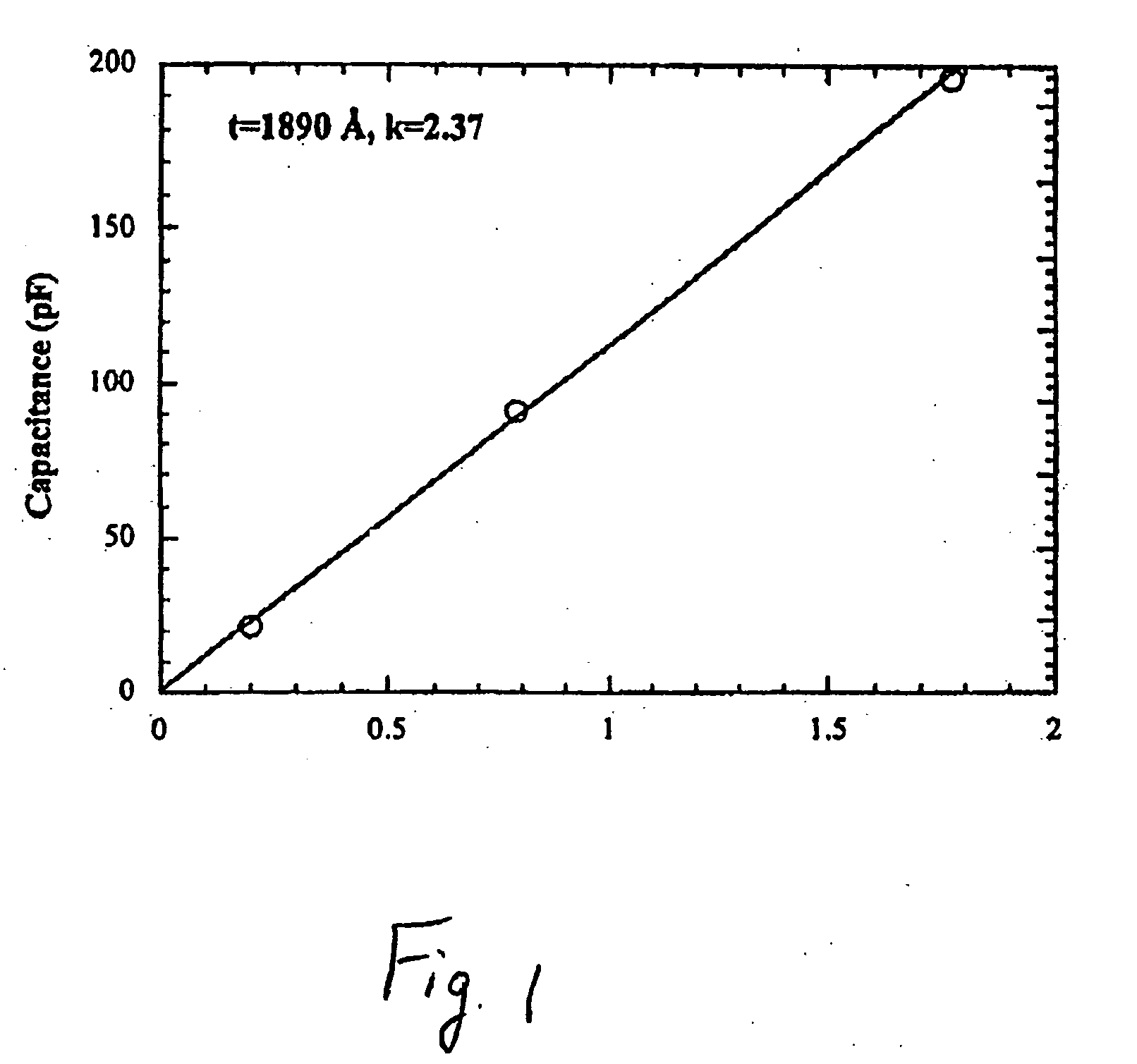
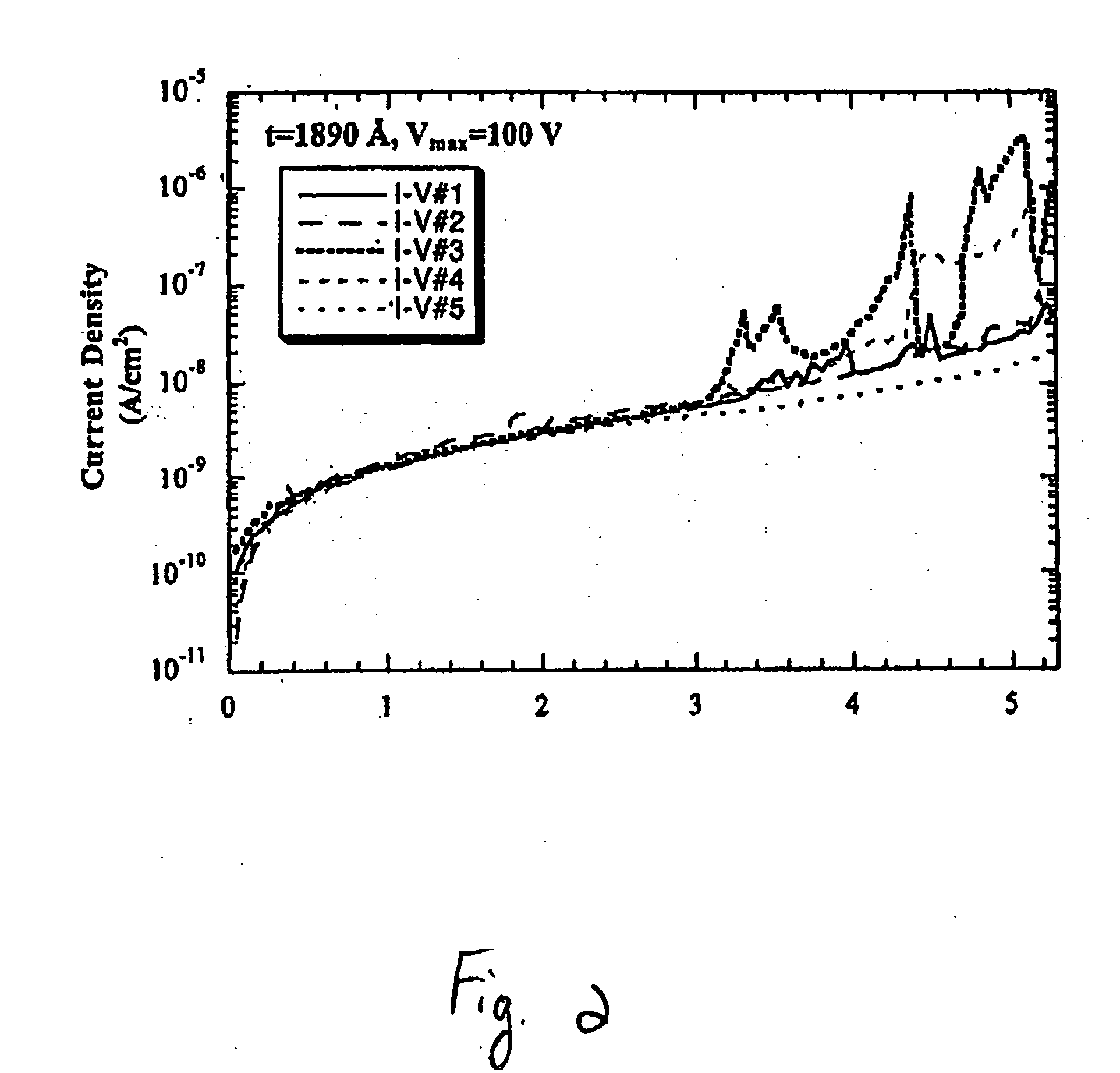
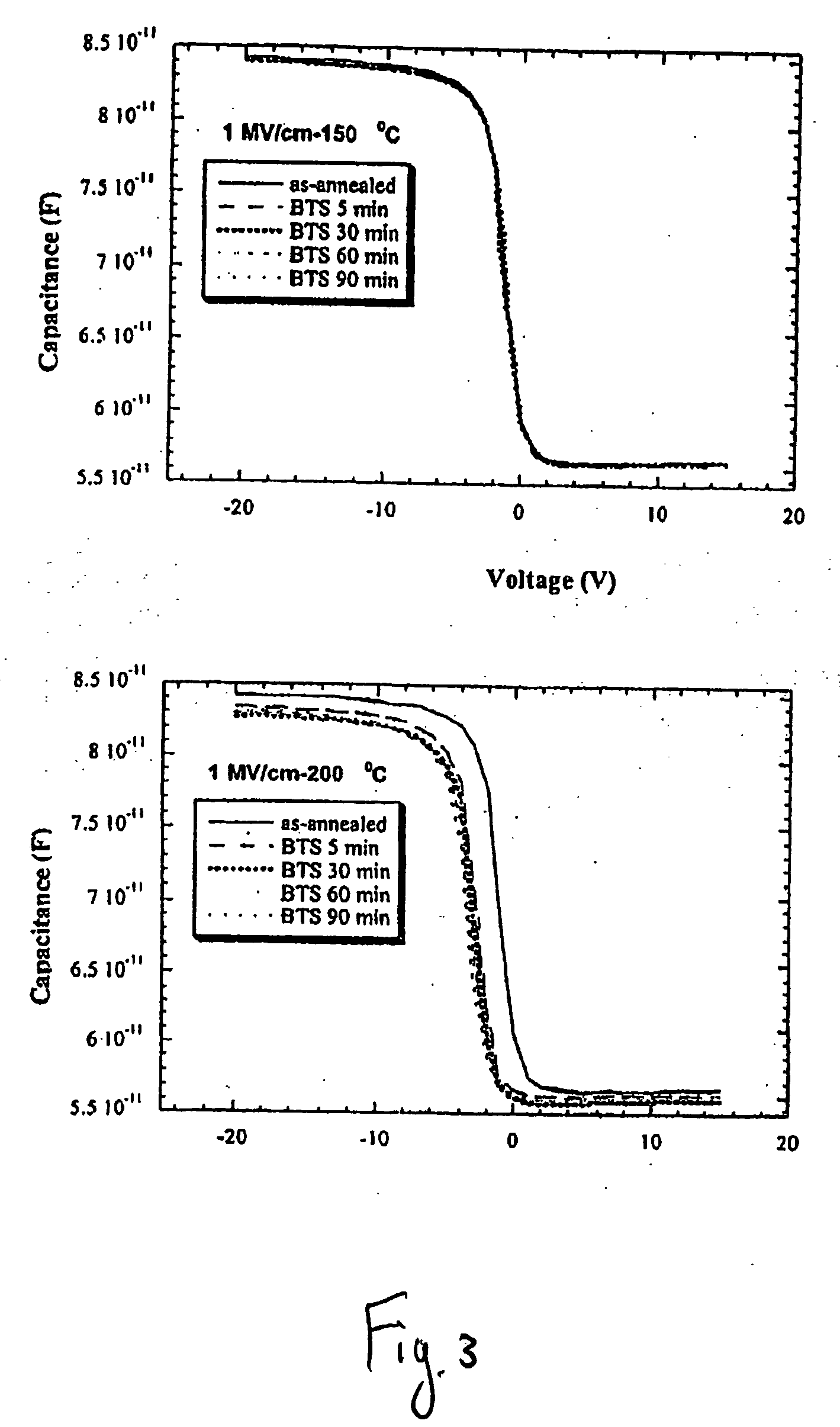
[0061] N type, 4-inch silicon wafers with resistivity of ≦0.02 ohm-cm were used as substrates. After RCA cleaning of the wafers, HMDS was spin-coated at 3000 rpm for 40 sec onto the wafers prior to deposition. The cyclolinear carbosilane polymer was dissolved in xylene at a concentration of 15-20%. The solutions were filtered through a 0.2 mm filter and then spin-deposited onto the pretreated wafers at 3000 rpm for 100 sec, followed by drying in an oven at 140° C. for 30 min. The sample was then placed in a tube furnace and flushed with nitrogen gas for approximately half an hour. The furnace temperature was ramped at a rate of 1.0 C / min to 300° C. in a nitrogen atmosphere and held a temperature for 8 hours before cooling to room temperature. The resultant films were used for electrical property measurements. The measurements demonstrated the use of the polymer films as an interlayer dielectric material and a capping layer. From her...


PUM


Abstract

Low dielectric compositions and methods of use thereof in integrated circuits are disclosed. The low dielectric compositions are derived from carbosilane polymers and oligomers containing imbedded sila- or disilacyclobutane rings and, after heating to induce cross-linking, may be used as an interlayer dielectric as well as a capping layer within an integrated circuit.

Description

CROSS-REFERENCE TO RELATED APPLICATION [0001] This application claims priority from U.S. Provisional Application Ser. No. 60 / 607,102, filed Sep. 3, 2004, the entire contents of which are incorporated herein by reference.FIELD OF THE INVENTION [0002] The invention relates to low dielectric compositions, methods of use thereof in integrated circuits. BACKGROUND OF THE INVENTION [0003] The growth of Integrated Circuit (IC) technology is primarily based on the continued scaling of devices to ever-smaller dimensions. Smaller devices provide higher packing density and higher operating speed. In the ultra-large-scale integration (ULSI) era, millions, and soon to be billions, of transistors on a chip must be interconnected to give desired functions. As minimum device features shrink below 0.25 microns, the increase in propagation delay, cross-talk noise and power dissipation of the interconnect structure become limiting factors. It is therefore, essential to reduce the interconnect capacita...

Claims


Application Information

Patent Timeline
IPC IPC(8): H01L21/31
CPCH01L21/3121H01L21/02282H01L21/02123
Inventor INTERRANTE, LEONARD V.WU, ZHIZHONGWANG, PEI-ILU, TOH-MING
Owner RENESSELAER POLYTECHNIC INST
Learn More