Pixel clock generating apparatus, optical writing apparatus using a pixel clock, imaging apparatus, and method for generating pixel clocks

a technology of generating apparatus and generating apparatus, which is applied in the direction of inking apparatus, visual presentation using printers, instruments, etc., can solve the problems of image quality degradation, image fluctuation, and image quality decline, and achieve the effect of reducing the adverse influence of light flux

Inactive Publication Date: 2003-04-10
RICOH KK
View PDF15 Cites 93 Cited by
  • Summary
  • Abstract
  • Description
  • Claims
  • Application Information

AI Technical Summary

Benefits of technology

[0025] It is still another object of the invention to provide a technique for correcting positional offset of dots, based on information obtained from two or more detectors in an efficient manner, while reducing adverse influence on light flux.
[0028] By giving phase data to a data block unit, the amount of correction data for dot offset can be greatly reduced, while flexibly and precisely correcting dot offset in the main scanning direction for each data block.
[0036] With this method, phase data for designating phase shift given to a pixel clock is given to each data block, and the amount of data required to correct dot offset in the main scanning direction can be greatly reduced.

Problems solved by technology

If the scanning rate fluctuates, dot positions formed on a sheet are offset from the correct positions in the main scanning direction, which results in image fluctuation and deteriorated image quality.
In this case, the displacement of the light spots of the respective color beams differ from each other on the scanned medium (e.g., the photosensitive unit), which causes the image quality to deteriorate.
It is difficult to correct the displacement or positional offset of light spots or dots because the fluctuation of the scanning rate itself varies along the scanning line due to the characteristics of the optical systems used in the imaging apparatus.
1) the f.theta. characteristic of the scanning lens is not sufficiently corrected
2) precision of the optical parts of the optical scanning system and assembling precision of the components onto the housing are insufficient;
3) the focal length changes due to deformation and change of the indexes of refraction of the optical components, which are caused by environmental changes, such as temperature change and humidity change, in the imaging apparatus;
4) the distance from the optical axis to the reflecting surface of the deflector (e.g., the polygonal mirror) varies, and the moving rate of the light spot on the scanned medium changes, as has been explained.
With this method, the clock signal fluctuates due to the influence of the frequency change during the lock-up time of the PLL, and consequently, the phase of the pixel clock cannot be precisely regulated.
Another problem in the prior art is that a huge amount of correction data is required to make correction to the entirety of image data when correcting the fluctuation of the scanning rate.
This problem causes the circuit scale to become large, and the cost for the control system also increases.
Still another problem is that if the phase of the pixel clock is corrected, without flexibility, based on the shift data, the corrected portions are repeated at the same positions in the sub-scanning direction, and vertical streaks appear in the resultant image.
There is yet another problem in the conventional optical writing system shown in FIG. 1B, which is separation of light flux.
To separate the light flux, the optical scanning system, including a deflector (e.g., a polygonal mirror) and other elements, inevitably becomes large.
In addition, separating a portion of the light flux from the light beam guided to the effective writing area deteriorates the detecting precision.
This problem becomes conspicuous especially in a multi-color imaging apparatus with multiple optical scanning systems.
However, errors that occur due to environmental changes as time passes, have to be measured and corrected during the operation of the apparatus.
This separation of light flux between the effective writing area and the detecting positions on the both sides is difficult.
However, it is more difficult for such a system to extract a portion of light flux in order to detect synchronization because of the layout design of arranging the optical scanning systems in the main scanning direction.

Method used


Image

  • Pixel clock generating apparatus, optical writing apparatus using a pixel clock, imaging apparatus, and method for generating pixel clocks
  • Pixel clock generating apparatus, optical writing apparatus using a pixel clock, imaging apparatus, and method for generating pixel clocks
  • Pixel clock generating apparatus, optical writing apparatus using a pixel clock, imaging apparatus, and method for generating pixel clocks

Examples


third embodiment

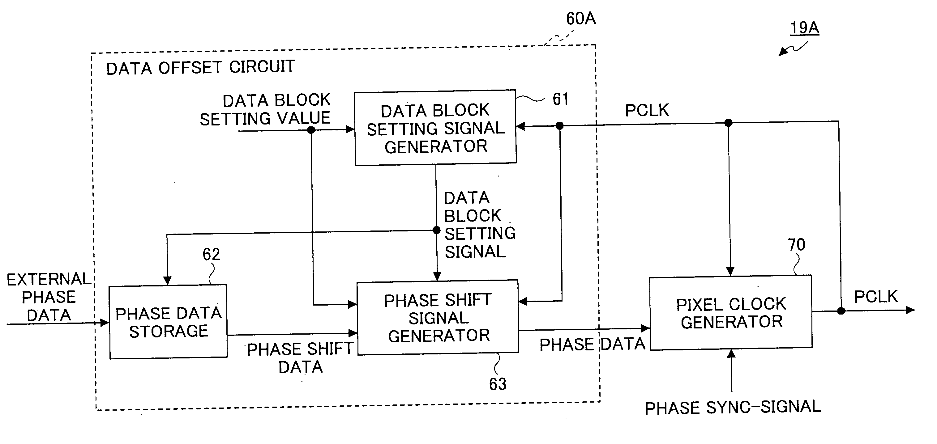
[0141] FIG. 16 illustrates a pixel clock generating unit 19C used in the optical writing apparatus 15 according to the invention. The same elements as those shown in FIG. 3 and FIG. 9 are denoted by the same numerical references, and explanation for them will be omitted. The pixel clock generating unit 19C comprises a pixel clock generator 70, and a data offset circuit 60C that defines multiple data blocks in the effective writing range and supplies appropriate phase data to the pixel clock generator 70. The pixel clock generator 70 has the same structure as that shown in FIG. 4A or FIG. 4B. The data offset circuit 60C includes a data block setting signal generator 61, a phase data storage 62, a phase shift signal generator 63, and a data block setting period signal generator 64. The data block setting period signal generator 64 generates a data block setting period signal based on the externally supplied data block setting value that defines the number of pixel clocks contained in ...

sixth embodiment

[0194] The dot offset detector / controller 110 produces second phase data for dynamic correction, in addition to first phase data for static correction. The first phase data is used repeatedly every line to correct dot offset due to statistic factors, such as the lens characteristic of the scanning lens. The second phase data is used to correct dot offset due to dynamic factors, such as fluctuation in rotational speed of the polygonal mirror that changes each line. In this case, the pixel clock generator 120 has a phase data composite circuit (not shown) to synthesize the first and second phase data. If the multi-beam light source structure described in the sixth embodiment is applied to the optical writing apparatus shown in FIG. 30, then multiple pairs of detectors 101 and 102 are furnished so as to simultaneously produce phase data for multiple lines corresponding to the respective light sources.

[0195] The pixel clock generator 120 generates a pixel clock based on the phase data s...

seventh embodiment

[0203] To overcome this problem, in the seventh embodiment, characteristic values representing the relation between the actual image height and the ideal image height of the optical scanning system in use are determined in advance by preliminary experiment or simulation to create a lookup table. The optical scanning time is successively measured during the actual printing operation using the optical writing apparatus. A correction amount required for correcting dot offset is obtained from the lookup table based on the measured scanning time, and appropriate phase shift amount is determined so that the dot position approaches the ideal position. With this arrangement, dot offset in the main scanning direction due to the environmental changes in the apparatus can be effectively corrected.


PUM


Abstract

A pixel clock generating apparatus comprises a data offset circuit and a pixel generator. The data offset circuit defines multiple data blocks, each data block consisting of a predetermined number of successive clocks, and produces phase data for each data block. The phase data represents an amount and a direction of phase shift to be carried out for a certain clock in each data block. The pixel generator receives the phase data from the data offset circuit and generates a phase-shifted pixel clock a predetermined number of times in each data block based on the phase data.

Description

[0001] 1. Field of the Invention[0002] The present invention relates to a technique for controlling the phase of a pixel clock to correct the positional offset of dots in an imaging apparatus, and to a technique for detecting a scanning beam in synchronization with optical writing to control the phase of the pixel clock.[0003] 2. Description of the Related Art[0004] FIGS. 1A and 1B schematically illustrate conventional imaging apparatuses. In FIG. 1A, a laser beam emitted from a semiconductor laser unit 1001 is reflected by a rotating polygonal mirror 1002 in a scanning direction, and focused by a scanning lens 1003 onto a photosensitive unit 1004. The focused laser beam forms a light spot and produces an electrostatic latent image on the photosensitive unit 1004. Laser driving circuit 1007 controls the light emission time of the semiconductor laser unit 1001, based on pixel data generated by an image processing unit 1006 and the pixel clock whose phases are determined by a phase sy...

Claims


Application Information

Patent Timeline
Patent Type & Authority Applications(United States)
IPC IPC(8): B41J2/47G02B26/12G06K15/12H04N1/053
CPCB41J2/471G02B26/122G06K15/1219H04N1/053H04N2201/04768H04N2201/02443H04N2201/04798
Inventor OMORI, ATSUFUMIISHIDA, MASAAKINIHEI, YASUHIROHAYASHI, YOSHINORI
Owner RICOH KK
Why Eureka
Try Eureka