Luminescence device and display apparatus
a technology of luminescent devices and display devices, which is applied in the direction of discharge tube luminescent screens, natural mineral layered products, etc., can solve the problems of material change or life deterioration, material change or deactivation process, and the efficiency of luminescence is limited to at most 25%, and achieves high luminescence efficiency, long device life, and high stability as luminescent materials.
- Summary
- Abstract
- Description
- Claims
- Application Information
AI Technical Summary
Benefits of technology
Problems solved by technology
Method used
Image
Examples
examples
[0173] Hereinbelow, the present invention will be described more specifically based on Examples.
examples 1 and 2
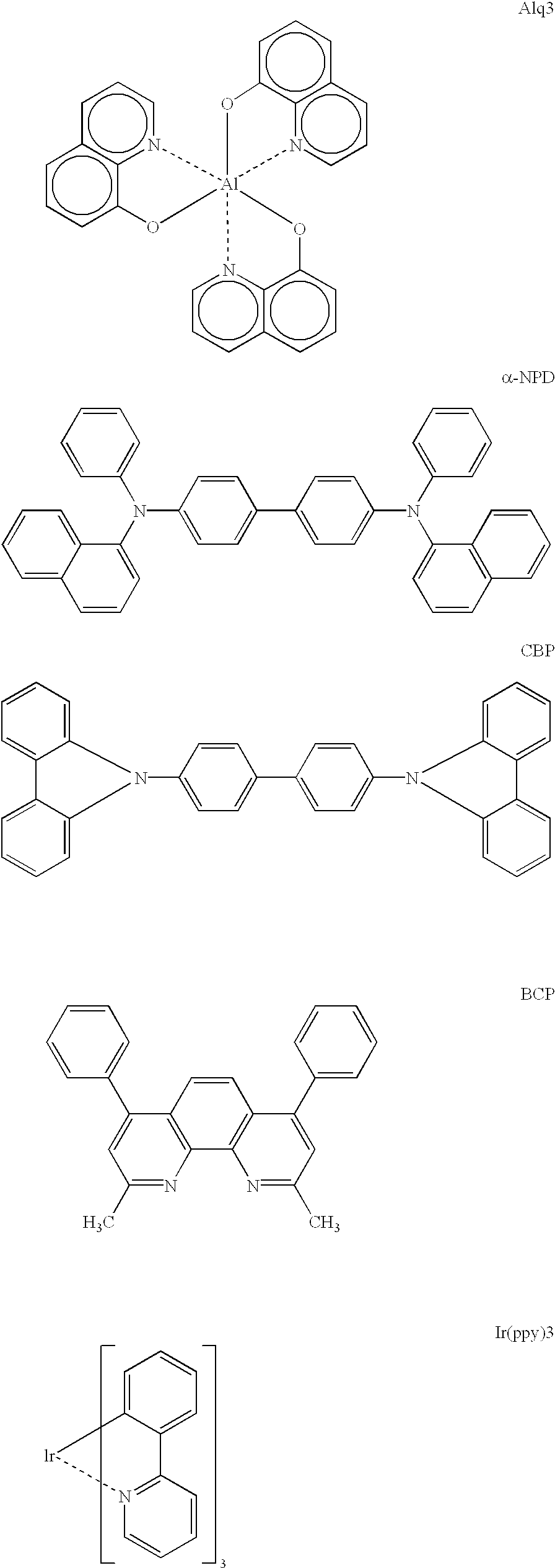
[0174] In these Examples, a device (effective display area=3 mm.sup.2) having a device structure including 4 organic layers as shown in FIG. 1(c) was prepared. An alkali-free glass sheet was used as a transparent substrate 15 and a 100 nm-thick indium oxide (ITO) film was formed by sputtering and patterned as a transparent electrode 14. Further, .alpha.-NPD represented by the above-mentioned structural formula was vacuum-deposited in a layer thickness of 40 nm thereon as a hole-transporting layer 13. Then, as an organic luminescence layer 12, the above-mentioned CBP as a host material and a prescribed metal coordination compound in an amount of providing 8 wt. % were co-vacuum deposited in a layer thickness of 30 nm. Further, as an exciton diffusion-prevention layer 17, BCP was vacuum-deposited in a thickness of 10 nm. Then, as an electron-transporting layer 16, the above-mentioned Alq3 was subjected to resistance heating vacuum deposition at a vacuum of 10.sup.-4 Pa to form an orga...
example 6
[0185] A simple matrix type organic EL device as shown in FIG. 2 was prepared in the following manner.
[0186] On a glass substrate 21 measuring 100 mm-length, 100 mm-width and 1.1 mm-thickness, a ca. 100 nm-thick ITO film was formed by sputtering and patterned into 100 lines of 100 .mu.m-wide transparent electrodes 22 (anode side) with a spacing of 40 .mu.m as simple matrix electrodes. Then, formed layers of identical organic materials were found under identical conditions as in Example 1 to form an organic compound layer 23.
[0187] Then, 100 lines of 100 .mu.m-wide Al electrodes 24 were formed with a spacing of 40 .mu.m by mask vacuum deposition so as to be perpendicular to the transparent electrodes 22 by vacuum deposition at a vacuum of 2.7.times.10.sup.-3 Pa. The metal electrodes (cathode) 24 were formed as a lamination of 10 nm-thick layer of Al / Li alloy (Li: 1.3 wt. %) and then 150 nm-thick layer of Al.
[0188] The thus-obtained 100.times.100-simple matrix-type organic EL device w...
PUM
| Property | Measurement | Unit |
|---|---|---|
| Fraction | aaaaa | aaaaa |
| Fraction | aaaaa | aaaaa |
| Fraction | aaaaa | aaaaa |
Abstract
Description
Claims
Application Information


