Sampling level converter circuit, 2-phase and multiphase expanding circuit, and display device

a converter circuit and multi-phase technology, applied in the direction of digital storage, electrical analogue stores, instruments, etc., can solve the problems of increasing the number of contacts of these numerous terminals, increasing the amount of power consumed, and the possibility of high voltage being applied to the input terminal, so as to reduce power consumption

Inactive Publication Date: 2003-04-24
VISTA PEAK VENTURES LLC
View PDF6 Cites 48 Cited by
  • Summary
  • Abstract
  • Description
  • Claims
  • Application Information

AI Technical Summary

Benefits of technology

0021] Accordingly, it is an object of the present invention to provide a level converter circuit having a fewer number of terminals and reduced power consumption, as well as a 2-phase and multiphase expanding circuit having such a level converter circuit.

Problems solved by technology

The problem that arises is a large number of connections (contacts) for these numerous terminals.
If a number of such levels converting circuits mounted, therefore, the amount of power consumed increases.
As a result, there is the possibility that a high voltage will be applied to the input terminal.

Method used


Image

  • Sampling level converter circuit, 2-phase and multiphase expanding circuit, and display device
  • Sampling level converter circuit, 2-phase and multiphase expanding circuit, and display device
  • Sampling level converter circuit, 2-phase and multiphase expanding circuit, and display device

Examples


first embodiment

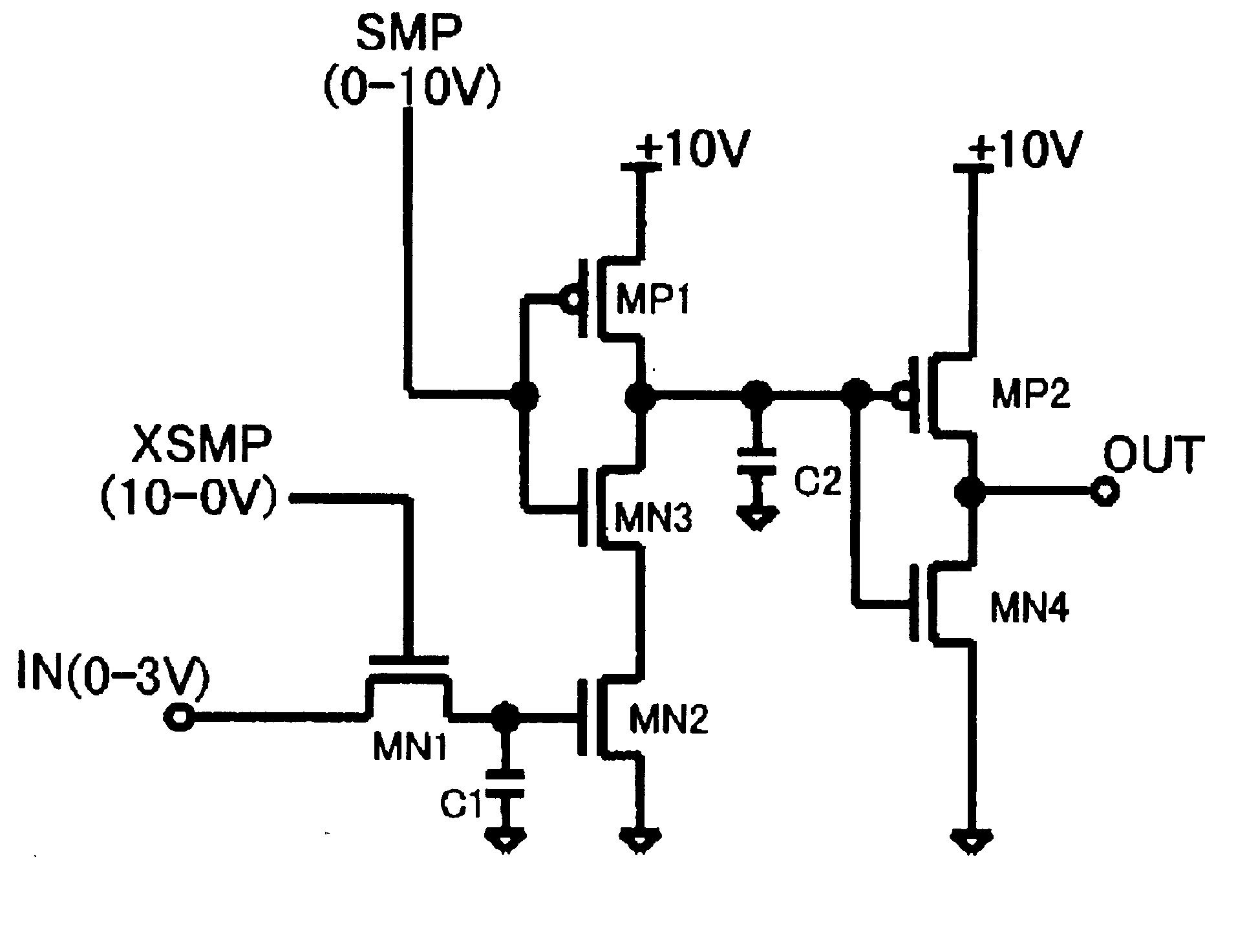
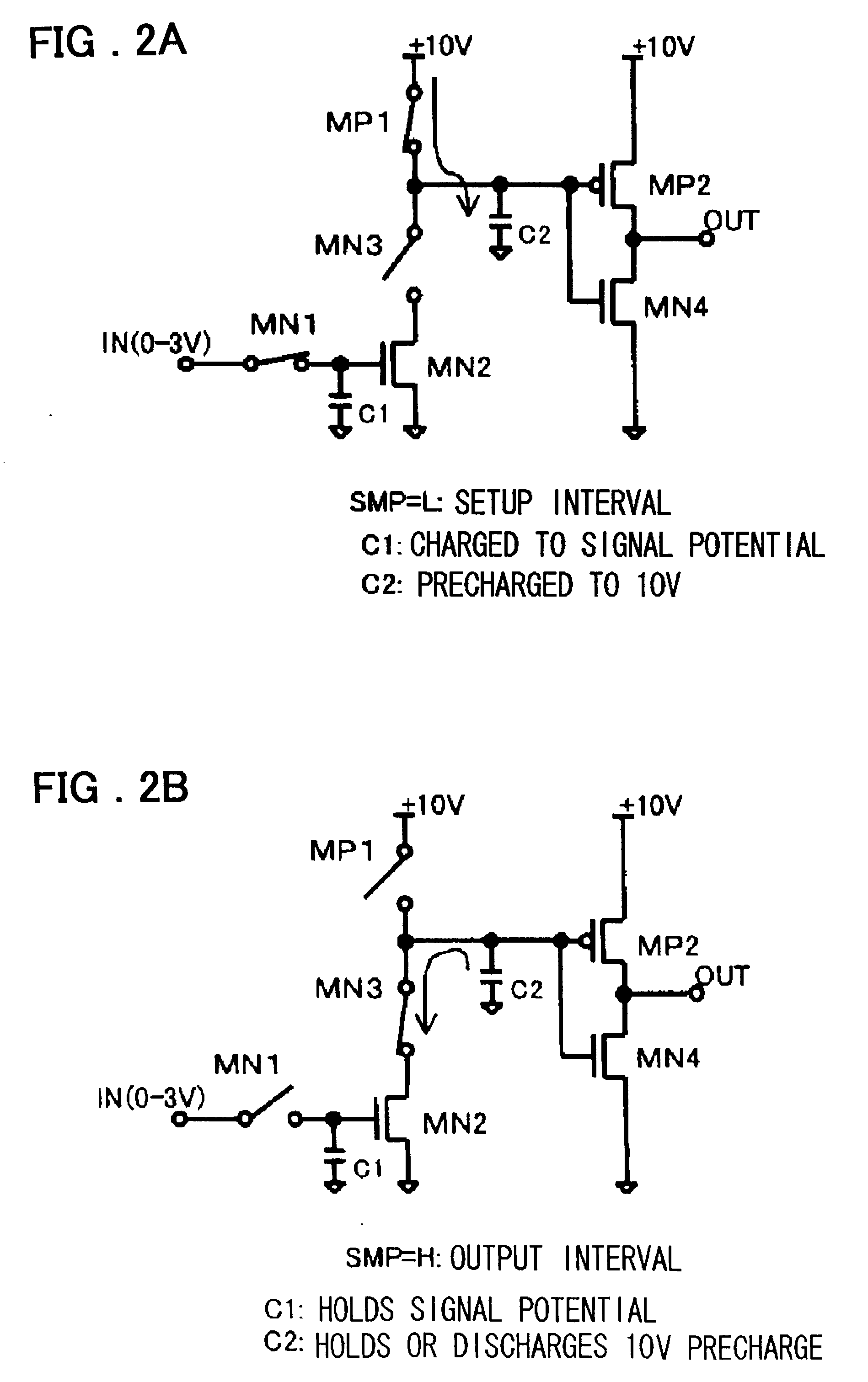
[0056] In the present invention, as shown in FIG. 1, a sampling level converter circuit includes means for turning on a switch element (transistor MP1 in FIG. 1), which has been inserted into a charging path (the path between a capacitor C2 and a higher-potential power-supply) of an output node, for a setup time-interval on the basis of sampling control signals (SMP, XSMP in FIG. 1) input thereto, thereby precharging the output node to the voltage of the higher-potential power-supply; and means (transistor MN1 and capacitor C1 in FIG. 1) for sampling an input signal voltage. The discharging path of the output node is set to an off (non-conductive) state (transistor MN3 in FIG. 2 is turned off) based upon the entered sampling control signal (SMP) in the setup time-interval. A switch element (a transistor MN2 in FIG. 1) that has been inserted into the discharging path of the output node is turned on or off in accordance with a logic value (the terminal voltage of the capacitor C1) of ...

third embodiment

[0107] the present invention will now be described with reference to FIG. 7, which is a diagram illustrating the structure of this embodiment. This diagram shows the structure of a circuit for expanding serial data to 2-phase data.

[0108] Two circuits, each of which is made up of a sampling level converter circuit, a plurality of inverters and a master / slave latch and has been described with reference to FIG. 3, are connected in parallel with respect to a single data input terminal DATA and a latch unit of a single stage is added onto one of these two circuit, whereby even-numbered input data and odd-numbered input data are output in parallel, in sync with the rising edge of the sampling pulse signal SMP, at a frequency obtained by dividing the frequency of the input data by 2. More specifically, as shown in FIG. 7, two sampling level converter circuits of the above-described embodiment are provided in parallel with respect to the data input terminal DATA. As shown in FIG. 7, the fir...


PUM


Abstract

Disclosed is a sampling level converter circuit having a fewer number of terminals and reduced power consumption, as well as an expanding circuit having such a sampling level converter circuit. The sampling level converter circuit includes first to third MOS transistors connected serially between a higher-potential power-supply and a lower-potential power-supply; a first capacitor connected to a connection node of the first and second MOS transistors; a fourth MOS transistor connected between an input terminal and the gate terminal of the third MOS transistor; and a second capacitor connected to the gate of the third MOS transistor. A sampling pulse signal is supplied to the gates of the first and second MOS transistors, and a signal obtained by inverting this sampling pulse signal is supplied to the gate of the fourth MOS transistor.

Description

[0001] This invention relates to a level converter circuit. The invention further relates to a sampling level converter suited for use in display devices such as a liquid crystal display device or electroluminescence (EL) display device, and to an expanding circuit equipped with the sampling level converter.[0002] In order to obtain liquid crystal display devices of smaller size, lower cost and higher resolution(definition), the development of techniques for integrating circuits provided within a liquid crystal display device (module) on the same substrate as that of the liquid crystal display substrate is proceeding apace. In one example known in the art, a driver circuit made up of polysilicon thin-film transistors (abbreviated below as "polysilicon TFT" or "p-Si TFT") is integrated on a liquid crystal substrate. One example of a method of forming a film of polysilicon TFT on a glass substrate or the like at low temperatures is to build up a precursor film under reduced pressure o...

Claims


Application Information

Patent Timeline
Patent Type & Authority Applications(United States)
IPC IPC(8): G09G3/20G09G3/30G09G3/36G11C19/18G11C27/02H03K19/0185
CPCG09G3/3688G09G2310/027H03K19/01855G11C19/184G11C27/024G09G2310/0289
Inventor HAGA, HIROSHI
Owner VISTA PEAK VENTURES LLC
Why Eureka
Try Eureka