

Method of forming insulating film and method of producing semiconductor device
- Summary
- Abstract
- Description
- Claims
- Application Information
AI Technical Summary
Benefits of technology
Problems solved by technology
Method used
Image

Examples
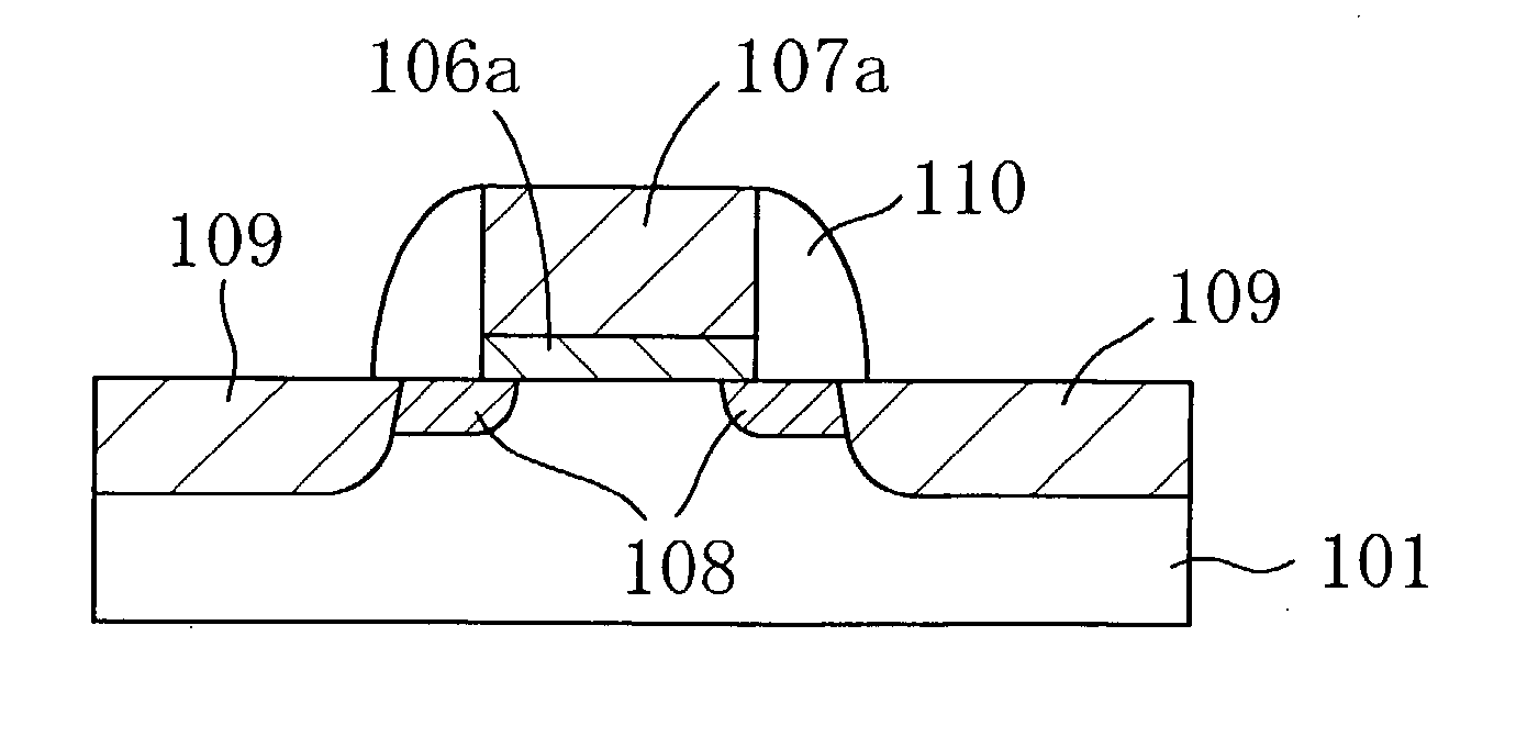
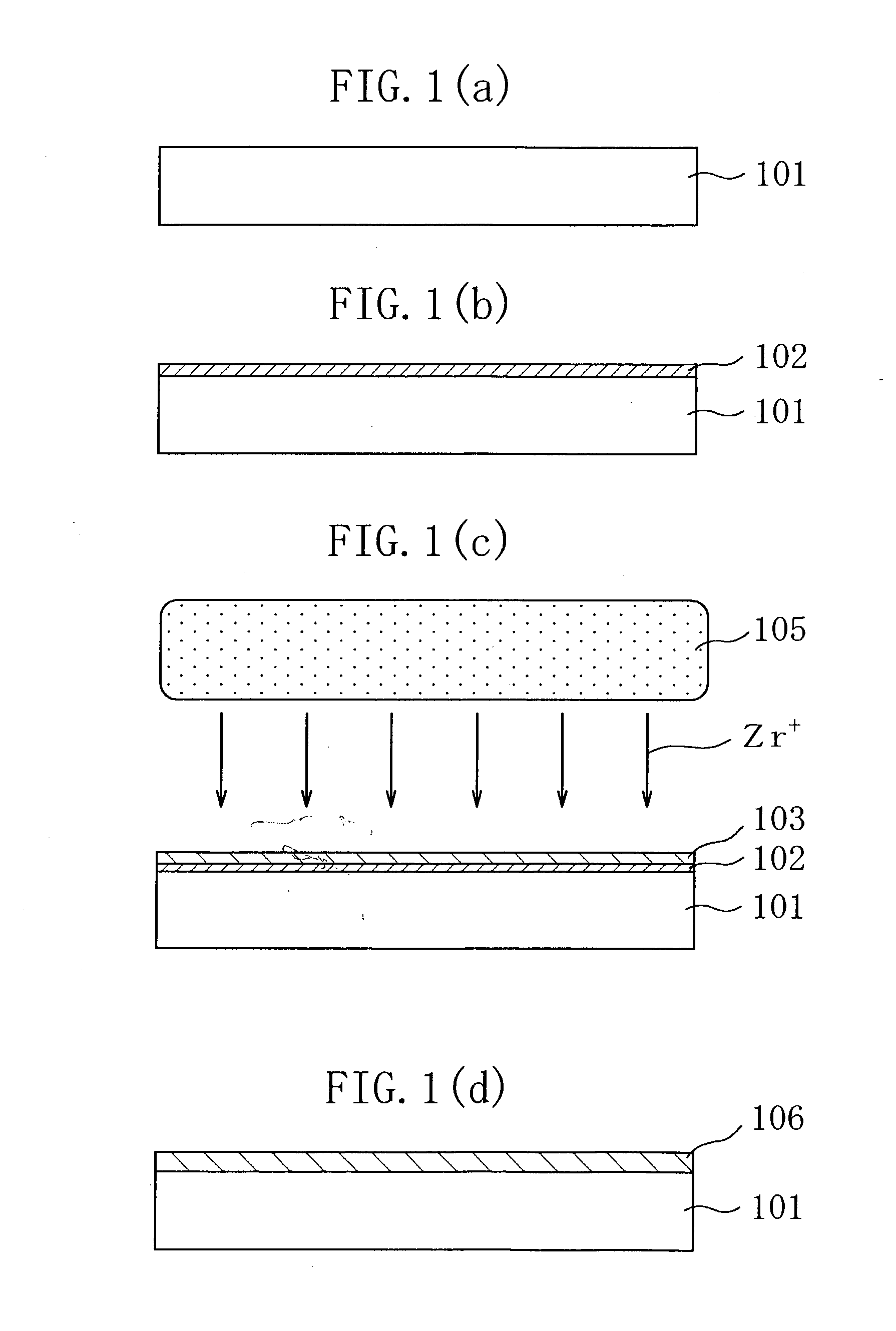
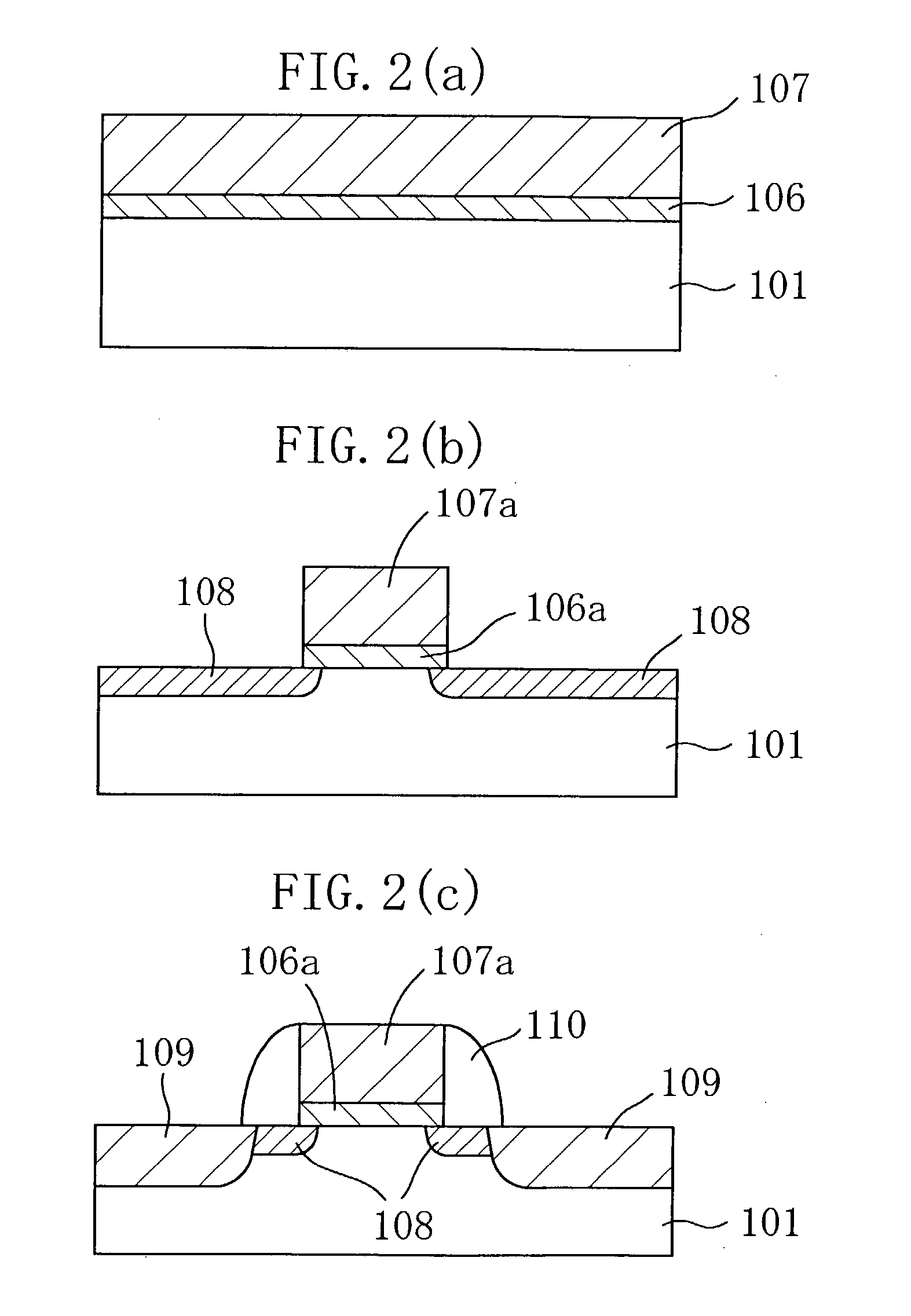
second embodiment
[0171] Furthermore, on the basis of the process steps of the second embodiment, the injection dose of Si ions that is to be introduced into a metal film formed on a silicon substrate is changed among the multiple regions located on the silicon substrate, and thereby the gate leakage properties and the high-peed operation characteristic of a resultant transistor can be traded off one against another.
fourth embodiment
[0172] Furthermore, on the basis of the process steps of the third or fourth embodiment, the injection dose of Si ions that is introduced into a metal film formed on a silicon substrate is changed among the multiple regions located on the silicon substrate, and thereby the gate leakage properties and the high-peed operation characteristic of a resultant transistor can be traded off one against another.
[0173] According to the methods for forming insulating films or the methods for fabricating semiconductor devices of the present invention, a high dielectric film is formed by utilizing ion implantation or plasma ion implantation, and heat treatment. Therefore, an insulating film which has a good interface state between the insulating film and the semiconductor substrate and which also has good leakage properties can be formed stably in a simple manner.
PUM
 Abstract
Description
Claims
Application Information