Data voltage current drive amoled pixel circuit

a data voltage current and amoled technology, applied in the field of pixels, can solve the problems of non-zero operating voltage of amorphous silicon, severe stress on the tft by higher voltage-time multiplier, and inability to drive the oleds with a current source comprised of nfets

Inactive Publication Date: 2003-05-22
INNOLUX CORP
View PDF13 Cites 230 Cited by
  • Summary
  • Abstract
  • Description
  • Claims
  • Application Information

AI Technical Summary

Problems solved by technology

Due to the manner in which the OLEDs are usually fabricated, i.e., having a common cathode for all pixels in the display, it is not normally possible to drive the OLEDs with a current source comprised of NFETs.
However, for driving OLEDs requiring nearly continuous current for operation, the amorphous silicon operating voltages are non-zero for a substantially larger percentage of the time (duty cycles up to 100%).
The higher voltage-time multiplier severely stresses the TFT.
A typical human observer can detect a pixel to pixel light output variation of as little as 1%, however, a level of 5% luminance variation is typically considered as being unacceptable.
AC voltages on TFT terminals tend to minimize effects of trapped charge and can prolong TFT lifetimes.
Since current is either sourced into or sunk out of the data or column line, the pixel circuits previously disclosed may not be suitable for high format displays.
The lower pixel currents may not be able to charge the column line in a line time due to the large capacitance.
However, the higher currents require higher voltage, and thus cause higher stress on the TFT.
The higher currents also increase power supply voltage drops and current return voltage drops.
At some point with increasing display format, this approach may not be practical.
In addition, current source or sink drivers for active matrix organic light emitting diodes (AMOLEDs) are not presently commercially available.
A problem is that although voltage data drivers are readily available, there are no amorphous silicon pixel circuits that can convert the voltage data to current for driving an OLED having a common cathode, without a threshold voltage dependence.
The circuit requires custom designed row drivers and the circuit does not appear to be suited for high-resolution displays.
The circuit requires custom design current data line drivers and the circuit dissipates a substantial amount of power as it incorporates two transistors in series to source current.
In addition, no previous pixel circuit or driving methods apply a multilevel voltage signal to a terminal of an OLED.

Method used


Image

  • Data voltage current drive amoled pixel circuit
  • Data voltage current drive amoled pixel circuit
  • Data voltage current drive amoled pixel circuit

Examples


Embodiment Construction

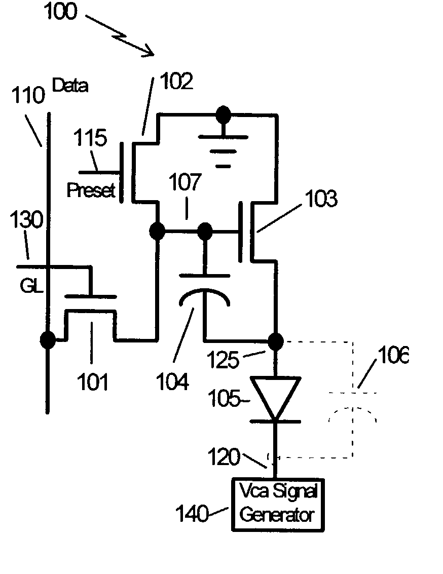
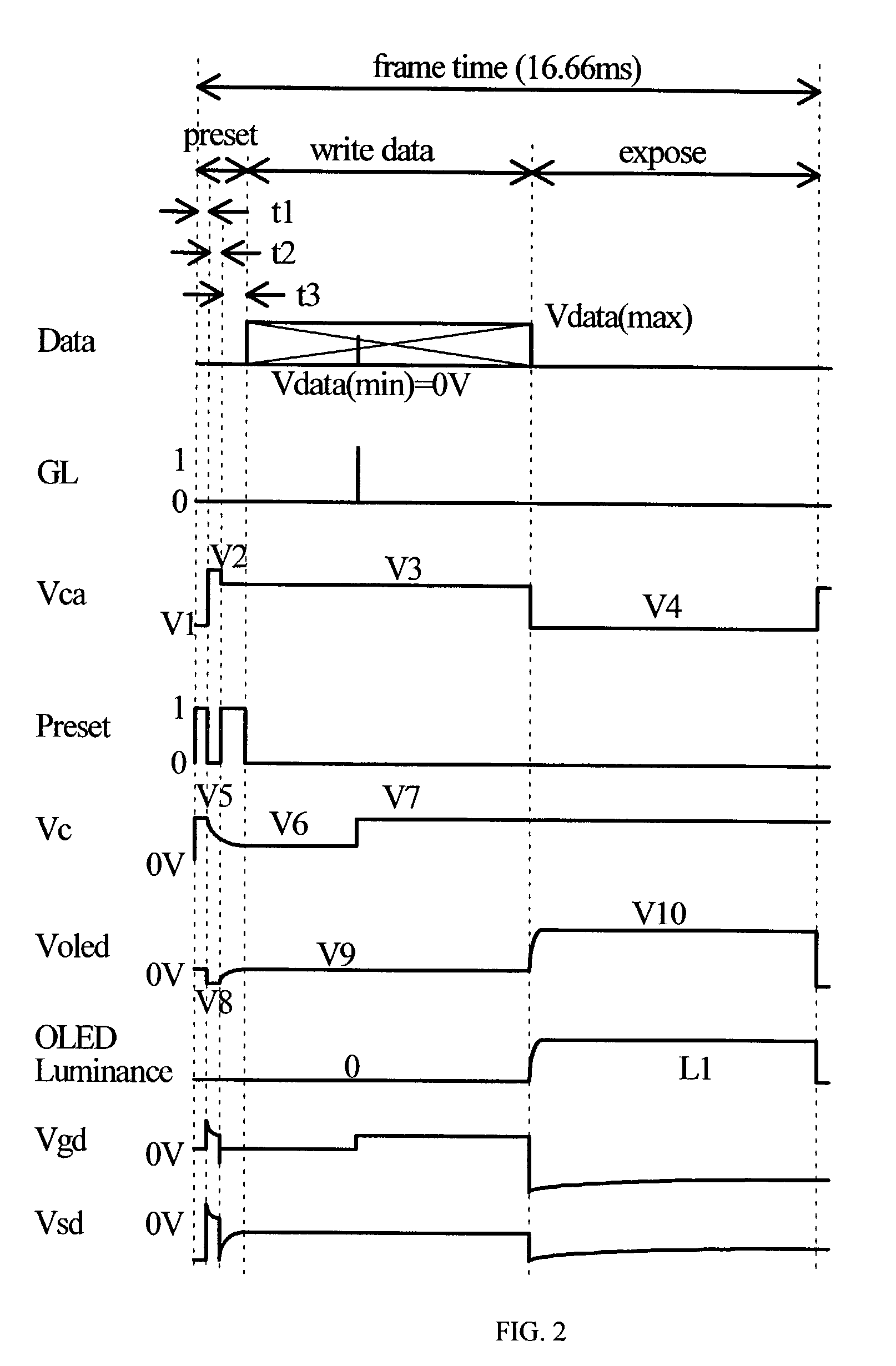
[0023] An embodiment of the present invention is a circuit for driving an OLED. In a frame time, there is a preset time interval, a write data time interval and an expose time interval. During the preset time interval, the circuit sets a preset voltage on a storage capacitor. The preset voltage is a threshold voltage of a current drive transistor that provides current to the OLED. During the write data time interval, data in the form of a data voltage is added to the preset voltage on the storage capacitor. During the expose time interval, the current provided by the current drive transistor is dependent only on the data voltage on the storage capacitor, and it is independent of threshold voltage of the current drive transistor.

[0024] FIG. 1 is a schematic diagram of an embodiment of circuit 100 for driving an OLED 105 in accordance with the present invention. Circuit 100 employs a method that includes providing a current to the anode of OLED 105, and applying a variable voltage sig...


PUM


Abstract

There is provided a circuit for driving an organic light emitting diode (OLED). The circuit includes a current source for providing current to a first terminal of the OLED, and a generator for providing a variable voltage signal to a second terminal of the OLED to facilitate control of the current.

Description

[0001] The present application is claiming priority of U.S. Provisional Patent Application Serial No. 60 / 331,913, filed on Nov. 20, 2001.[0002] 1. Field of the Invention[0003] The present invention relates to a pixel circuit, and more particularly, to a data voltage current-drive OLED pixel circuit. The circuit establishes a threshold voltage of a current drive transistor operating in saturation across a storage capacitor. Thereafter, the circuit writes a data voltage into the storage capacitor for controlling current through the OLED.[0004] 2. Description of the Prior Art[0005] One method to achieve large size OLED (organic light emitting diode) displays is to use an active matrix thin film transistor (TFT) backplane. An active matrix consists of an array of rows and columns of pixels each having an active device such as a transistor. Row lines driven by row drivers are sequentially selected, one row line at a time, from top to bottom, while data for a selected row is presented on ...

Claims


Application Information

Patent Timeline
Patent Type & Authority Applications(United States)
IPC IPC(8): G09G3/32
CPCG09G3/3233G09G2300/0819G09G2320/043G09G2300/0866G09G2310/0254G09G2300/0842
Inventor LIBSCH, FRANK R.SANFORD, JAMES L.
Owner INNOLUX CORP
Why Eureka
Try Eureka