Semiconductor nanocrystal probes for biological applications and process for making and using such probes

a technology of micro-crystal probes and nano-crystals, applied in scanning probe techniques, fluorescence/phosphorescence, instruments, etc., can solve the problem of difficult simultaneous or even non-simultaneous detection or discrimination between the presence of a number, and the limitation of the number of different color organic dye molecules which may be utilized simultaneously or sequentially

Inactive Publication Date: 2003-05-29
WEISS SHIMON +2
View PDF16 Cites 66 Cited by
  • Summary
  • Abstract
  • Description
  • Claims
  • Application Information

AI Technical Summary

Problems solved by technology

There are a number of problems with such an analytical system.
As a result, there is a severe limitation on the number of different color organic dye molecules which may be utilized simultaneously or sequentially in an analysis since it is difficult to either simultaneously or even non-simultaneously detect or discriminate between the presence of a number of different detectable substances due to the broad spectrum emissions and emission tails of the labeling molecules.
Another problem is that most dye molecules have a relatively narrow absorption spectrum, thus requiring either multiple excitation beams used either in tandem or sequentially for multiple wavelength probes, or else a broad spectrum excitation source which is sequentially used with different filters for sequential excitation of a series of probes respectively excited at different wavelengths.
Another problem frequently encountered with existing dye molecule labels is that of photostability.
In addition, the probe tools used for the study of systems by electron microscopy techniques are completely different from the probes used for study by fluorescence.
Thus, it is not possible to label a material with a single type of probe for both electron microscopy and for fluorescence.
Both of these properties of dyes impair the ability to use a plurality of differently colored dyes when exposed to the same energy source.
However, since the semiconductor nanocrystals are inorganic, they may not bond directly to the affinity molecule.
Thus, exposure of a material to radiation (to which radiation the material is transparent) may result in local heating within the material.

Method used


Image

  • Semiconductor nanocrystal probes for biological applications and process for making and using such probes
  • Semiconductor nanocrystal probes for biological applications and process for making and using such probes
  • Semiconductor nanocrystal probes for biological applications and process for making and using such probes

Examples


example 2

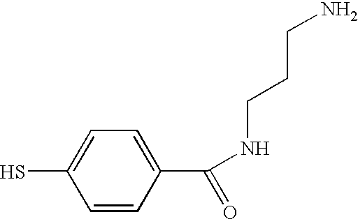
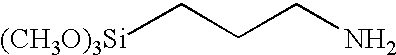
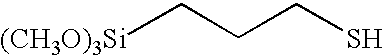
[0125] To illustrate the formation of a semiconductor nanocrystal compound (comprising silica coated semiconductor nanocrystals linked to a linking agent) 200 .mu.l of 3-(mercaptopropyl)-trimethoxysilane and 40 .mu.l of 3-(aminopropyl)-trimethoxysilane were added to 120 ml of anhydrous 25% (v / v) dimethylsulfoxide in methanol. The pH of this solution was adjusted to 10 using 350 .mu.l of a 25% (w / w) solution of (CH.sub.3).sub.4)NOH in methanol. 10 mg of CdS or ZnS or ZnS / CdS coated CdSe nanocrystals were dissolved into this solution (prepared, in the case of CdS, by a technique such as the technique described in the aforementioned Peng, Schlamp, Kadavanich, and Alivisatos article; or in the case of ZdS, by the technique described by Dabbousi et al. in "(CdSe)ZnS Core-Shell Quantum Dots: Synthesis and Characterization of a Size Series of Highly Luminescent Nanocrystals," Journal of Physical Chemistry B 101 pp 9463-9475, 1997), stirred to equilibrate for several hours, diluted with 200...


PUM

PropertyMeasurementUnit
sizeaaaaaaaaaa
heightaaaaaaaaaa
wavelengthsaaaaaaaaaa

Abstract

A semiconductor nanocrystal compound is described which is capable of linking to one or more affinity molecules. The compound comprises (1) one or more semiconductor nanocrystals capable of, in response to exposure to a first energy, providing a second energy, and (2) one or more linking agents, having a first portion linked to the one or more semiconductor nanocrystals and a second portion capable of linking to one or more affinity molecules. One or more of these semiconductor nanocrystal compounds are linked to one or more affinity molecules to form a semiconductor nanocrystal probe capable of bonding with one or more detectable substances in a material being analyzed, and capable of, in response to exposure to a first energy, providing a second energy. In one embodiment, the probe is capable of emitting electromagnetic radiation in a narrow wavelength band and / or absorbing, scattering, or diffracting energy when excited by an electromagnetic radiation source (of narrow or broad bandwidth) or a particle beam. The probe is stable to repeated exposure to energy in the presence of oxygen and / or other radicals. Treatment of a material with the semiconductor nanocrystal probe, and subsequent exposure of this treated material to a first energy, to determine the presence of the detectable substance within the material bonded to the probe, will excite the semiconductor nanocrystal in the probe bonded to the detectable substance, causing the probe to provide a second energy signifying the presence, in the material, of the detectable substance bonded to the semiconductor nanocrystal probe. In one embodiment, the semiconductor nanocrystals in the probe are excitable over a broad bandwidth of energy, and emit electromagnetic radiation over a narrow bandwidth, making it possible to use a single energy source to simultaneously excite a plurality of such probes, each emitting electromagnetic radiation of a differing wavelength band to simultaneously analyze for a plurality of detectable substances in a material being analyzed. Also described are processes for respectively making the semiconductor nanocrystal compound and the semiconductor nanocrystal probe. Processes are also described for treating materials with the probe, for example, to determine the presence of a detectable substance in the material bonded to the probe.

Description

[0001] This application is a continuation in part of U.S. patent application Ser. No. 08 / 978,450 filed Nov. 25, 1997, and assigned to the assignee of this application.[0002] The invention described herein arose in the course of, or under, Contract No. DE-AC03-SF00098 between the United States Department of Energy and the University of California for the operation of the Ernest Orlando Lawrence Berkeley National Laboratory. The Government may have rights to the invention.[0003] 1. Field of the Invention[0004] This invention relates to semiconductor nanocrystal probes for biological applications wherein the probes include a plurality of semiconductor nanocrystals capable of providing a detectable signal in response to exposure to energy.[0005] 2. Description of the Related Art[0006] Fluorescent labeling of biological systems is a well known analytical tool used in modem bio-technology as well as analytical chemistry. Applications for such fluorescent labeling include technologies such...

Claims


Application Information

Patent Timeline
Patent Type & Authority Applications(United States)
IPC IPC(8): C12Q1/68C12Q1/6816G01N21/64G01N33/533G01N33/542G01N33/543G01N33/58G01Q70/08G01Q70/18
CPCB82Y15/00Y10T436/141111C09K11/565C09K11/883C09K11/89C09K11/892C12Q1/6816G01N33/533G01N33/542G01N33/54373G01N33/588C09K11/025Y10T436/142222H01L33/0062H01L33/0083C12Q2563/107
Inventor WEISS, SHIMONBRUCHEZ, MARCELALIVISATOS, PAUL
Owner WEISS SHIMON
Why Eureka
Try Eureka