Differential circuit, amplifier circuit, driver circuit and display device using those circuits

a technology of driver circuit and output, which is applied in the direction of gated amplifier, static indicating device, instruments, etc., can solve the problems of reducing and affecting the output output output, so as to reduce the deviation of the amplitude difference and reduce power consumption

Active Publication Date: 2003-08-28
RENESAS ELECTRONICS CORP
View PDF4 Cites 83 Cited by
  • Summary
  • Abstract
  • Description
  • Claims
  • Application Information

AI Technical Summary

Benefits of technology

0028] Accordingly, it is an object of the present invention to provide a differential circuit and an amplifier circuit capable of performing full range drive and reducing power consumption while reducing an amplitude difference deviation.

Problems solved by technology

However, this type of driver circuit, if used in the driver circuit of a liquid crystal display device, would generate an output deviation in the output of each of the two amplifiers because of variations in the transistor characteristic.
Therefore, the problem is that, when the two-voltage follower circuits 910 and 920 are changed over to perform drive, the offset of the driver circuit in FIG. 15 varies greatly.
However, when the driver circuit shown in FIG. 15 is used as the amplifier circuit for amplifying the grayscale level voltage of a liquid crystal display device, the problem is that, when the two voltage follower circuits 910 and 920 are changed over for drive, the output offset varies greatly with the result that the grayscale level voltage interval cannot be kept constant.
However, a high-speed drive cannot be performed in the vicinity of the low-potential power supply VSS because the charge operation is performed by the current source 927, nor in the vicinity of the high-potential power supply VDD because the discharge operation is performed by the current source 917.
Therefore, a voltage cannot be speedily driven in an arbitrary order.

Method used


Image

  • Differential circuit, amplifier circuit, driver circuit and display device using those circuits
  • Differential circuit, amplifier circuit, driver circuit and display device using those circuits
  • Differential circuit, amplifier circuit, driver circuit and display device using those circuits

Examples


first embodiment

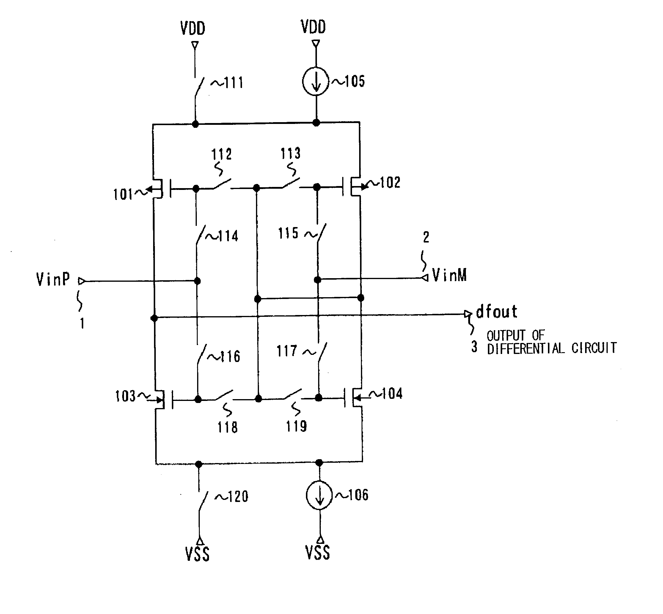
[0138] Some examples of the present invention will be described with reference to the drawings to describe more in detail the embodiments of the present invention described above. FIG. 1 is a diagram showing the configuration of the present invention.

[0139] Referring to FIG. 1, a differential circuit in this embodiment comprises a pair of p-channel transistors 101 and 102 and a pair of n-channel transistors 103 and 104. The sources of the paired p-channel transistors 101 and 102 are coupled together and, between the commonly coupled sources of the paired p-channel transistors and the high-potential power supply VDD, there are provided a switch 111 and a constant-current source 105 which are connected in parallel. Switches 112 and 113 are connected in series between the gates of the paired p-channel transistors 101 and 102. The drains of the p-channel transistor pair 101 and 102 are connected to the drains of the paired n-channel transistors 103 and 104.

[0140] The sources of the n-ch...

second embodiment

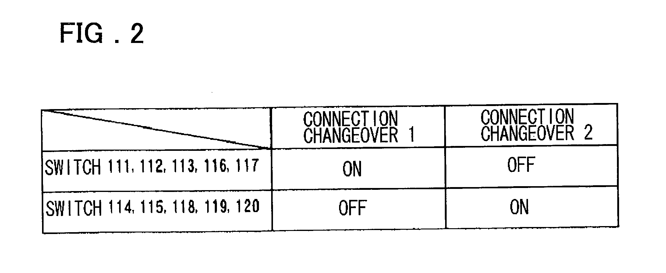
[0161] FIG. 4 is a diagram showing the configuration of the present invention. This figure shows an example of the configuration of the differential circuit shown in FIG. 1 in which the switches are configured by MOS transistors. In FIG. 4, switch control signals S1 and S2 are controlled by the low level (L) or high level (H).

[0162] The circuit enters the connection changeover 1 state by controlling the signals such that (S1, S2)=(H,L), and the circuit enters the connection changeover 2 state by controlling the signals such that (S1, S2)=(L,H). S1B and S2B are the inverted signals of S1 and S2.

[0163] Each switch may be any switch that may be connected and disconnected. FIG. 4 shows the configuration that requires less transistors (reduction in the number of devices) and less space. First, a switch 111 and a switch 120, one end of which is connected to the high-potential power supply VDD and the low-potential power supply VSS, may be configured respectively by a single p-channel tran...

third embodiment

[0168] Next, another embodiment of the present invention will be described. FIG. 5 is a diagram showing the configuration of the present invention. FIG. 5 shows the configuration of a driver circuit configured by using the differential circuit in FIG. 1. That is, a differential circuit in FIG. 5, which comprises transistors 101, 102, 103, and 104, switches 111-120, and current sources 105 and 106, is the same as the one shown in FIG. 1. FIG. 6 shows an example of how the driver circuit in FIG. 5 is controlled.

[0169] Referring to FIG. 5, this driver circuit is a feedback type amplifier circuit including two amplification stages 510 and 520 that operate in response to an output from the differential circuit shown in FIG. 1. Referring to FIG. 5, an input voltage Vin (input voltage VinP in FIG. 1) and an output voltage Vout (input voltage VinM in FIG. 1) are sent to the two input terminals (differential input terminals) of the differential circuit.

[0170] The amplification stage 510 is a...


PUM


Abstract

A differential circuit and an amplifier circuit for reducing an amplitude difference deviation, performing a full-range drive, and consuming less power are disclosed. The circuit includes a first pair of p-type transistors and a second pair of n-type transistors. A first current source and a first switch are connected in parallel between the sources of the first pair of transistors, which are tied together, and a power supply VDD. A second current source and a second switch are connected in parallel between the sources of the second pair of transistors, which are tied together, and a power supply VSS. The circuit further includes connection changeover means that performs the changeover of first and second pairs between a differential pair that receives differential input voltages and a current mirror pair that is the load of the differential pair. When one of the two pairs is the differential pair, the other is the current mirror pair. In a differential amplifier circuit, there is provided an added transistor connected in parallel to a transistor, which is one transistor of a differential pair transistors, whose control terminal is a non-inverting input terminal. The added transistor has a control terminal for receiving a control voltage which is set so that, when an input voltage applied to the non-inverting input terminal is in a range in which the transistor whose control terminal is the non-inverting input terminal is turned off, the added transistor is turned on.

Description

[0001] The present invention relates to a differential circuit, an amplifier circuit, a driver circuit and a display device using the circuit.[0002] A driver circuit is known that performs drive by changing over between a charging amplifier and a discharging amplifier for the full range drive on the high-potential side and the low-potential side. However, this type of driver circuit, if used in the driver circuit of a liquid crystal display device, would generate an output deviation in the output of each of the two amplifiers because of variations in the transistor characteristic. This increases the variation (termed as amplitude difference deviation) among outputs as to the voltage amplitude difference between the positive and negative polarities for the same grayscale level, sometimes resulting in degraded image quality. The amplitude difference deviation, one of performance characteristic of a multiple-output liquid crystal driver circuit, means a deviation in the outputs of the ...

Claims


Application Information

Patent Timeline
Patent Type & Authority Applications(United States)
IPC IPC(8): G09G3/20G09G3/36H03F3/45H03F3/72
CPCG09G3/2011G09G3/3685G09G2310/0291H03F2203/45616H03F3/72H03F2203/45506H03F3/45183
Inventor TSUCHI, HIROSHI
Owner RENESAS ELECTRONICS CORP
Why Eureka
Try Eureka