

Magnetic sensing element comprising antiferromagnetic layer laminated on free magnetic layer
a magnetic sensing element and antiferromagnetic layer technology, applied in the field of magnetic sensing elements, can solve the problems of generating lattice defects, unable to fully display the function of the magnetic sensing element, and suffering from the free magnetic layer
- Summary
- Abstract
- Description
- Claims
- Application Information
AI Technical Summary
Problems solved by technology
Method used
Image

Examples
Embodiment Construction
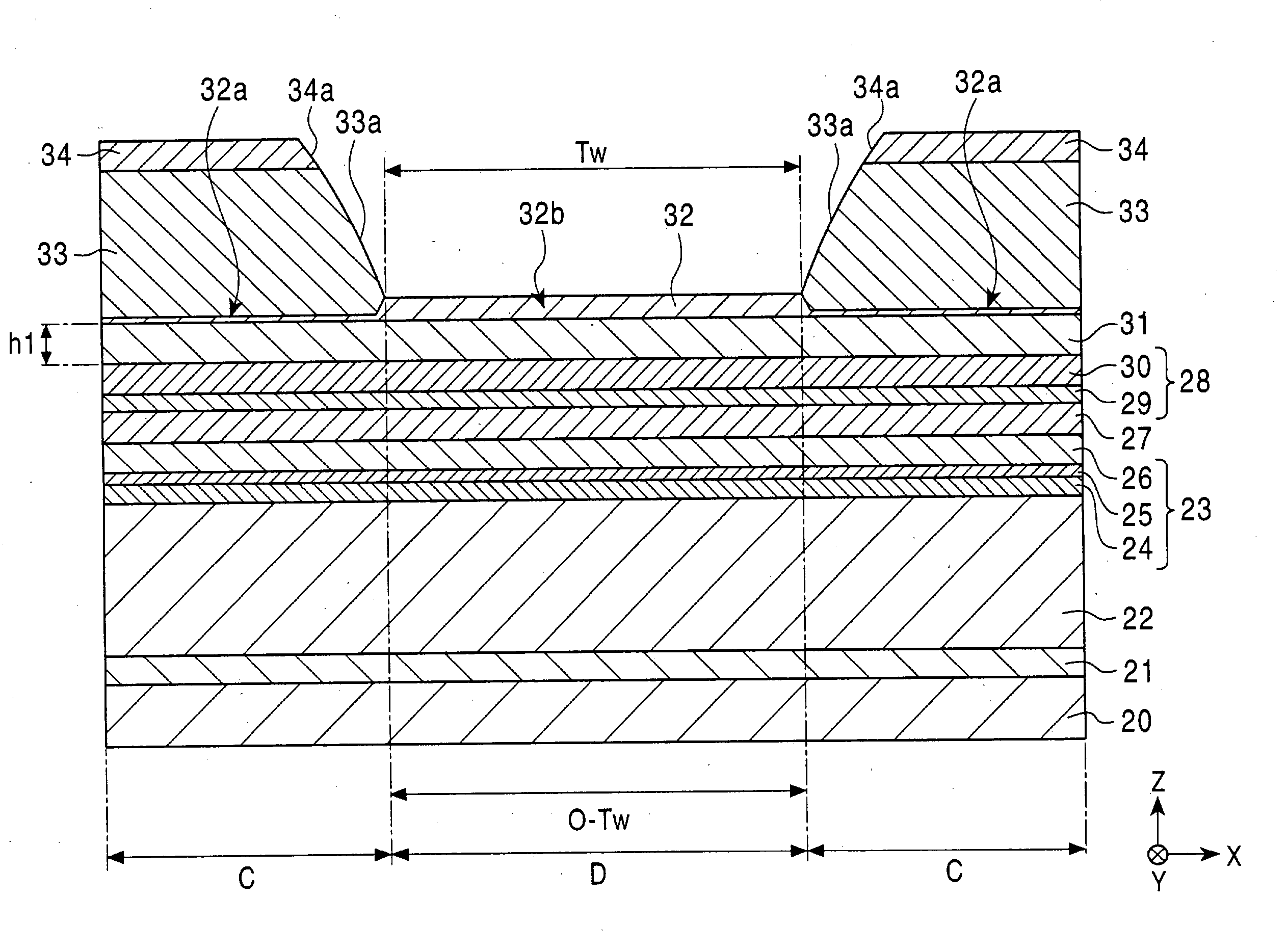
[0482] FIG. 27 is a graph showing the relation between the optical track width O-Tw and output of the sensed magnetic field in the exchange bias magnetic sensing element.
[0483] The output of the sensed magnetic field was measured by changing the optical track width O-Tw using three kinds of exchange bias magnetic sensing elements having the layer structure shown in FIG. 1 in which the materials of the magnetic material layer 30 of the free magnetic layer 28 are different with each other.
[0484] The height MRh of the element was adjusted to 0.75 times the optical track width O-Tw, and the thickness of the free magnetic layer was adjusted depending on the materials of the magnetic material layer 30 so that the magnetic moment Mst per unit area of the free magnetic layer is a constant value of 0.46 memu / cm2 (5.8 T.multidot.nm).
[0485] In the graph in FIG. 27, the dotted line connecting the marks (.diamond.) indicates the results when the magnetic material layer 30 of the free magnetic la...
PUM
| Property | Measurement | Unit |
|---|---|---|
| distance | aaaaa | aaaaa |
| width | aaaaa | aaaaa |
| width | aaaaa | aaaaa |
Abstract
Description
Claims
Application Information