So too are the problems inherent in combining different materials.
Principal amongst those problems is that of
thermal expansion coefficient differences because the
thermal expansion mismatch between
silicon, the primary material of interest for large-scale high-density integrated circuits, and III-V compounds, the materials of interest for optoelectronic and
microwave devices and circuits, is very large.
Such large mismatches make it difficult to grow device-quality III-V heterostructures directly on
silicon wafers, or to bond full wafers of III-V devices with full
silicon integrated circuit wafers.
This approach becomes limiting because the lattice structure of GaAs mismatches that of silicon.
In addition, growing GaAs onto silicon is inherently difficult and therefore costly.
Accordingly, GaAs or InP cannot efficiently be grown on a silicon substrate.
However, for the most part, heterogeneous integration today is done by using some variation of flip-
chip solder-ball (or solder-bump) bonding to attach modest size arrays of, for example, vertical-cavity surface emitting lasers (VCSELs) on individual
integrated circuit chips.
This approach works, but it also has serious limitations.
In particular, the size of the device array that can be bonded depends on the bonding temperature, and is typically limited to a
centimeter on a side.
However, severe limitations exist on the shape, size, and distribution of the components.
Furthermore, the structures disclosed by Yando typically possess
millimeter-sized dimensions and are therefore generally incompatible with micron sized integrated circuit structures.
Accordingly, the method and structure disclosed by Yando is thereby too large and complicated to be effective for assembling a state-of-art
microstructure or component onto a substrate.
Such a process is limiting because of the need for the human or
robotics arm.
The human or
robotics arm assembles each packaged device onto the substrate one-by-one and not simultaneously, thereby limiting the efficiency and effectiveness of the operation.
Moreover, the method uses
centimeter sized devices (or packed surface
mount integrated circuits), and would have little applicability with micron sized integrated circuits in die form.
A limitation to the method includes an apparatus capable of vibrating the structures, or an apparatus for pulsating air through the apertures.
Moreover, the method described relies upon
centimeter-sized dies and would have little applicability with state-of-art micron sized structures.
The method becomes limiting because of the need for a shaking apparatus for the electromagnetic shaking step.
Moreover, the method is solely in context to
electrode pedestals and silicon wafers, thereby limiting the use of such method to these structures.
A limitation with such method includes providing an apparatus capable of vibrating particles with electrostatic forces.
Moreover, the method of Cohn creates damage to a portion of the integrated circuits by mechanically vibrating them against each other and is also generally ineffective.
Accordingly the method typically becomes incompatible with a state-of-art
microstructure.
A limitation with such method is the lack of a mechanism to keep the trapezoidal shaped GaAs blocks in the inverted trapezoidal shaped recessed regions of the surface once the GaAs blocks are aligned with the recesses.
As the
slurry moves over the surface of the silicon wafer, the trapezoidal shaped GaAs blocks may disengage from the inverted trapezoidal shaped recessed regions and become part of the
slurry again, thereby reducing the effectiveness of this approach.
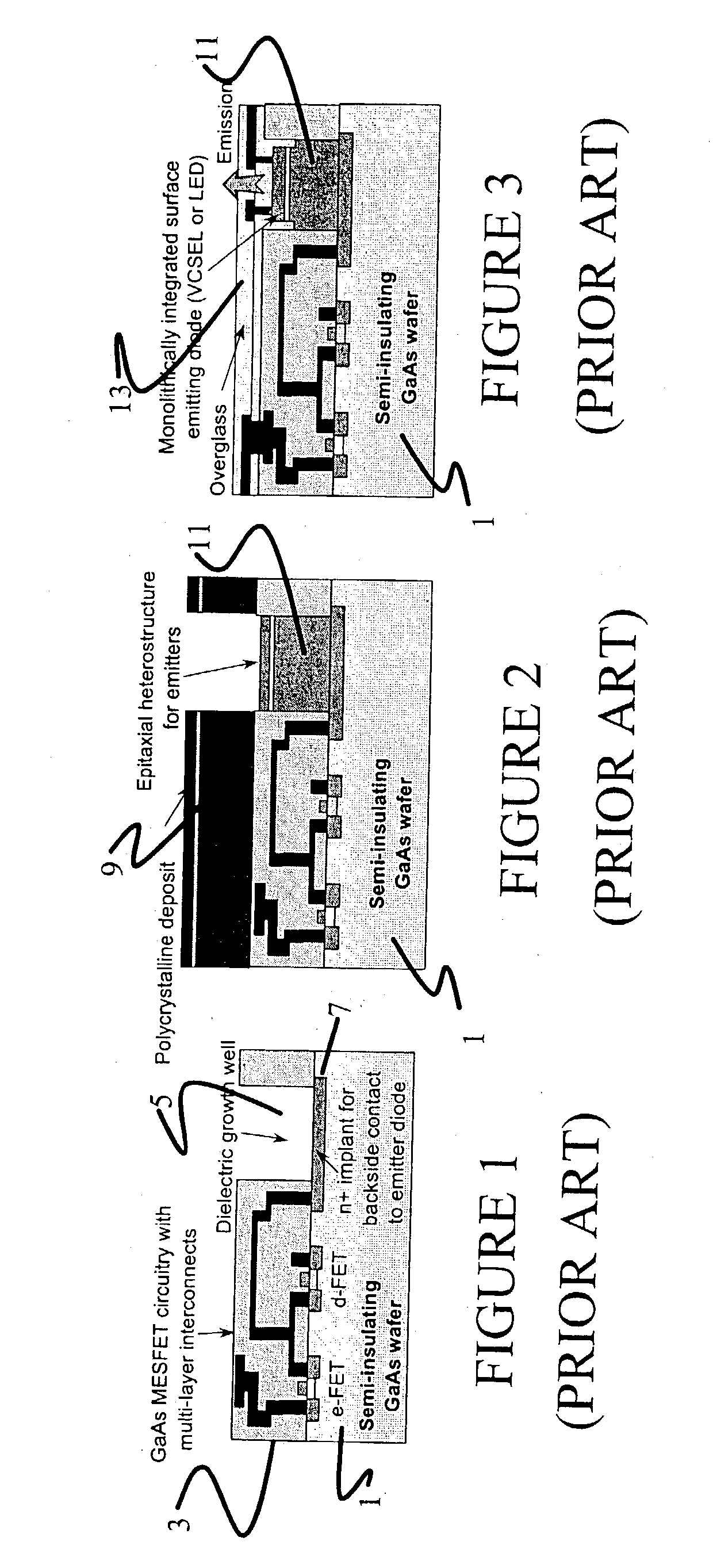
First, it requires
epitaxy on the integrated circuit substrate, which, as a practical matter, means that
Epitaxy-on-
Electronics cannot be used with silicon integrated circuits for the majority of heterostructure devices of interest.
The
epitaxy must also be done at less than 500.degree. C. to avoid damaging the preexisting
electronics, and this, and the semi-insulating IC substrate itself, can place a limitation on
material quality.
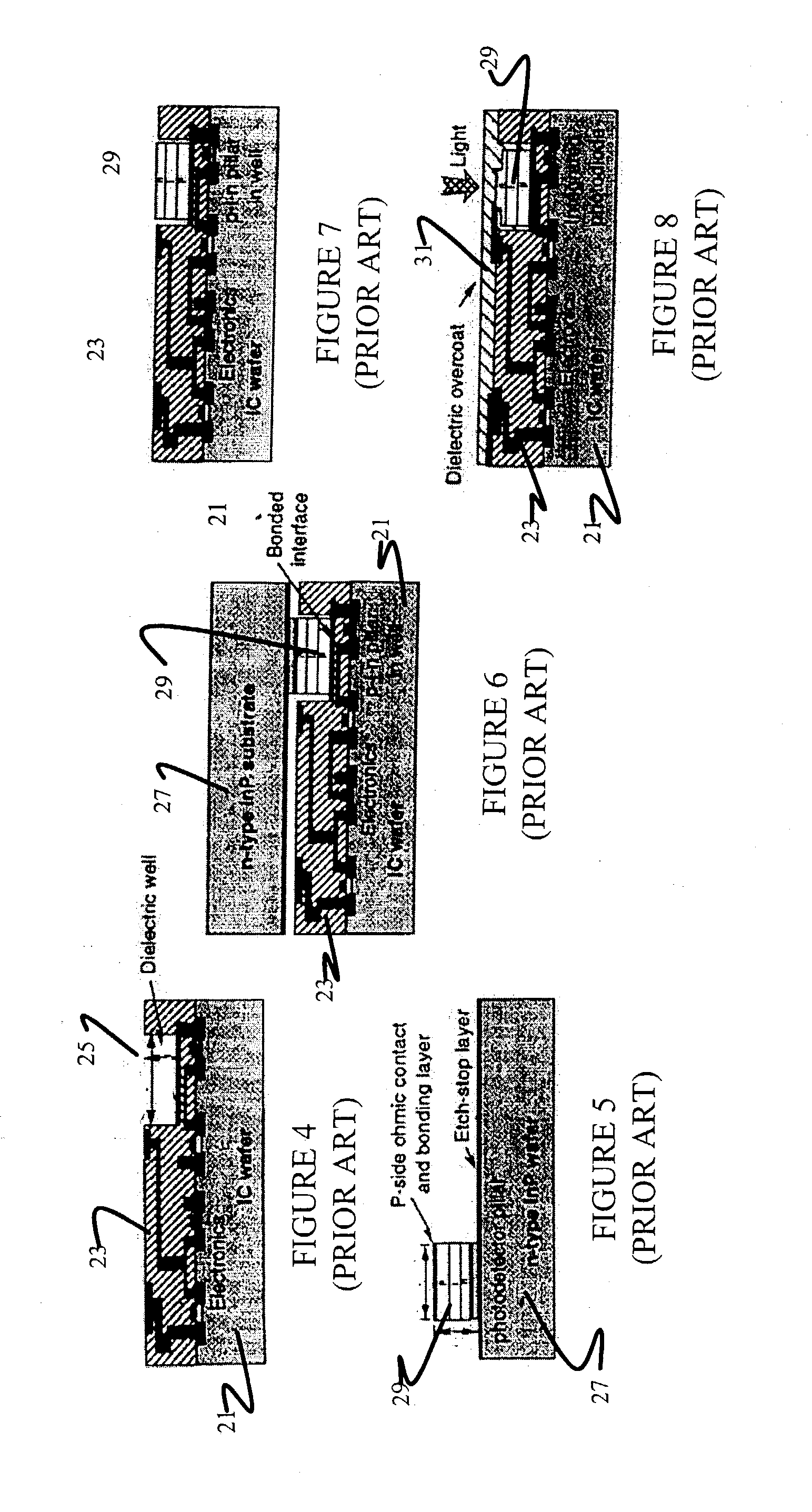
Aligned pillar
bonding process thus does allow access to silicon circuitry, but it does not take
advantage of the very large
diameter Si wafers that are available because it is limited by the
diameter of the heterostructure substrate.
It also, of course, can only be used with standard silicon
CMOS, for example, if used on partial wafers.

