Doped semiconductor wafer of float zone pulled semiconductor material, and process for producing the semiconductor wafer

a technology of float zone and semiconductor material, which is applied in the direction of crystal growth process, polycrystalline material growth, chemistry apparatus and processes, etc., can solve the problems of neutron doping with a large number of drawbacks, increase in dislocation rate, and reduction in process stability

Inactive Publication Date: 2003-10-16
SILTRONIC AG
View PDF4 Cites 14 Cited by
  • Summary
  • Abstract
  • Description
  • Claims
  • Application Information

AI Technical Summary

Problems solved by technology

A drawback of these measures is that they often lead to an increase in the dislocation rate and to a reduction in the process stability.
However, neutron doping has a large number of drawbacks.
For example, the method is only suitable for semiconductor material with a resistance of approximately 3 to approximately 800 Ohm*cm.
Radiation damage which has to be annealed by a thermal aftertreatment is inevitably produced.
Nevertheless, it is impossible to prevent a reduction in the minority charge carrier life.
Furthermore, necessary decay times, the thermal aftertreatment and associated conveying operations make the method time-consuming and expensive.
Secondly, particles which originate from the stock ingot also pass to the growth front together with the flow, where they have an adverse effect on the dislocation-free growth of the single crystal.
Furthermore, the technical problems increase, on account of the inevitably higher voltages.

Method used


Image

  • Doped semiconductor wafer of float zone pulled semiconductor material, and process for producing the semiconductor wafer
  • Doped semiconductor wafer of float zone pulled semiconductor material, and process for producing the semiconductor wafer
  • Doped semiconductor wafer of float zone pulled semiconductor material, and process for producing the semiconductor wafer

Examples


Embodiment Construction

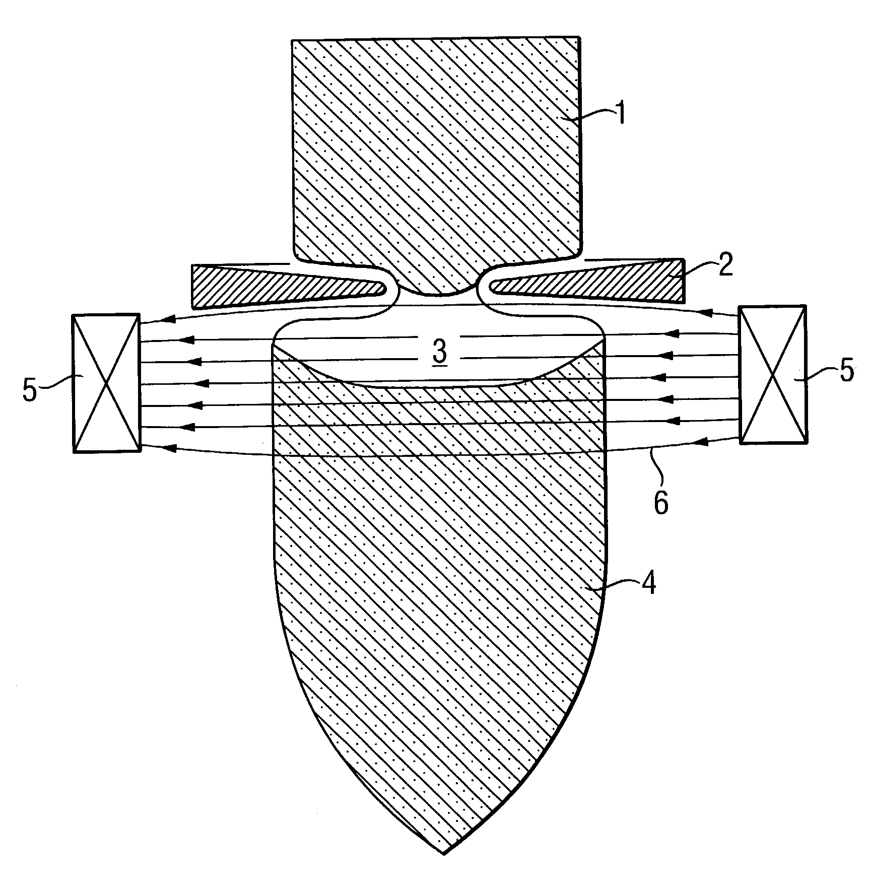
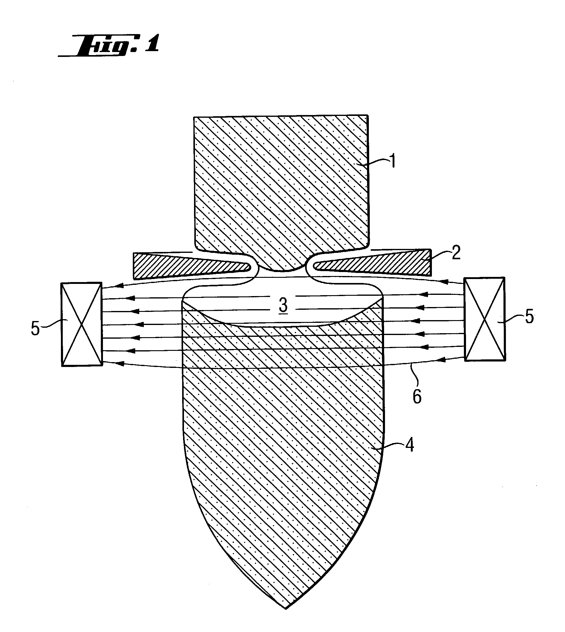
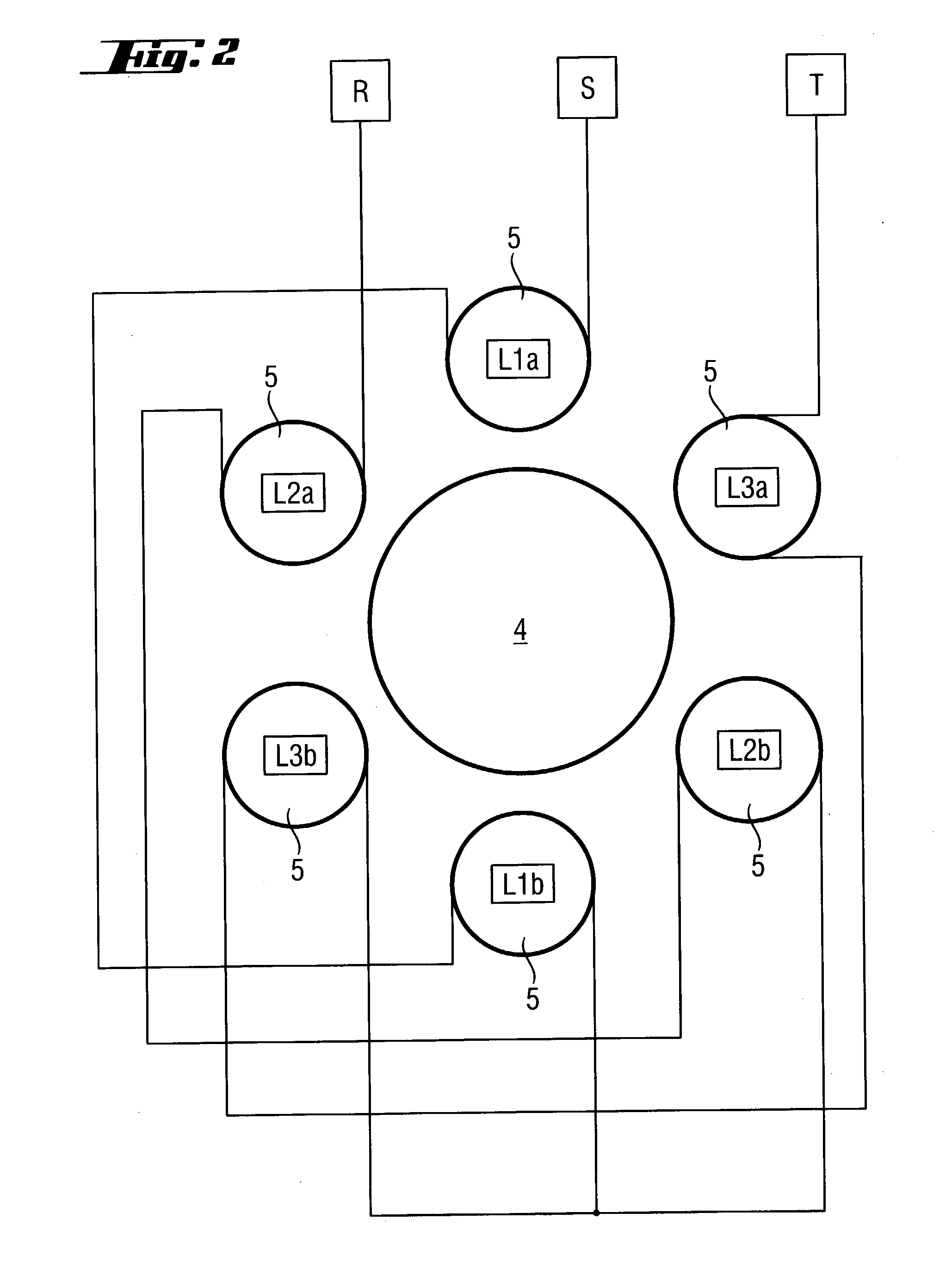
[0034] Silicon single crystals with a diameter of 4 inches were pulled using the FZ method. Some of the single crystals were pulled using a rotating magnetic field in accordance with the invention, while in others the magnetic field was not used. Then, silicon wafers which had been cut from the single crystals were examined for the distribution of dopants. FIG. 5 shows the resistance scatter and profile position for silicon wafers which originate from an FZ single crystal pulled using a rotating magnetic field in accordance with the invention.

[0035] FIG.6 shows a comparative illustration of measurements of the spreading resistance values. FIG. 6a shows the values for material which has been pulled using a rotating magnetic field in accordance with the invention, while FIG. 6b shows the values for material in which the rotating magnetic field was not used.

[0036] Accordingly, while a few embodiments of the present invention have been shown and described, it is to be understood that ma...


PUM

PropertyMeasurementUnit
magnetic fieldaaaaaaaaaa
resistanceaaaaaaaaaa
frequencyaaaaaaaaaa

Abstract

A doped semiconductor wafer of float zone-pulled semiconductor material contains a dopant added to a molten material and has a radial macroscopic resistance distribution of less than 12% and striations of -10% to +10%. There is also a process for producing a doped semiconductor wafer by float zone pulling of a single crystal and dividing up the single crystal, in which process, during the float zone pulling, a molten material which is produced using an induction coil is doped with a dopant. It is exposed to at least one rotating magnetic field and is solidified. The single crystal which is formed during the solidification of the molten material is rotated. The single crystal and the magnetic field are rotated with opposite directions of rotation and the magnetic field has a frequency of 400 to 700 Hz.

Description

[0001] 1. Field of The Invention[0002] The invention relates to a doped semiconductor wafer of float zone-pulled semiconductor material and to a process for producing the semiconductor wafer. The process comprises the production of a doped single crystal by float zone pulling (floating zone crystal growth, FZ method) and the division of the single crystal into semiconductor wafers. During the pulling of the single crystal, a molten material which has been produced using an induction coil is exposed to at least one rotating magnetic field and is solidified. The single crystal which is formed during the solidification of the molten material is rotated.[0003] 2. The Prior Art[0004] The use of a rotating magnetic field in float zone pulling is described, for example, in DD-263 310 A1. However, the process which is proposed in this document attempts to make the diffusion boundary layer thickness more uniform. However the present invention achieves the most homogeneous distribution of dop...

Claims


Application Information

Patent Timeline
Patent Type & Authority Applications(United States)
IPC IPC(8): C30B13/12C30B13/00C30B13/10C30B13/26C30B29/06
CPCC30B13/10C30B29/06C30B13/26
Inventor KNOBEL, ROLFAMMON, WILFRIED VONVIRBULIS, JANISGRUNDNER, MANFRED
Owner SILTRONIC AG
Why Eureka
Try Eureka