Puddle etching method of thin film by using spin-processor

Inactive Publication Date: 2003-10-23
GRAND PLASTIC TECH
View PDF5 Cites 31 Cited by
  • Summary
  • Abstract
  • Description
  • Claims
  • Application Information

AI Technical Summary

Problems solved by technology

The batch method do not suitable to large diameter wafers, the single wafer spin etch is suitable to diameter above 8 inches.
However, supplying etching solution to the spinning wafer will waste a lot of etching solution, the uniformity is not good enough, the rea

Method used


Image

  • Puddle etching method of thin film by using spin-processor
  • Puddle etching method of thin film by using spin-processor
  • Puddle etching method of thin film by using spin-processor

Examples


Embodiment Construction

[0013] Preferred embodiment of the present invention will now be explained with reference to the accompanying drawings. The preferred embodiment of the present invention made use of etching silicon dioxide as an example by using a spin processor of UFO-200 made by Grand plastic Technology Corporation to perform the puddle etching.

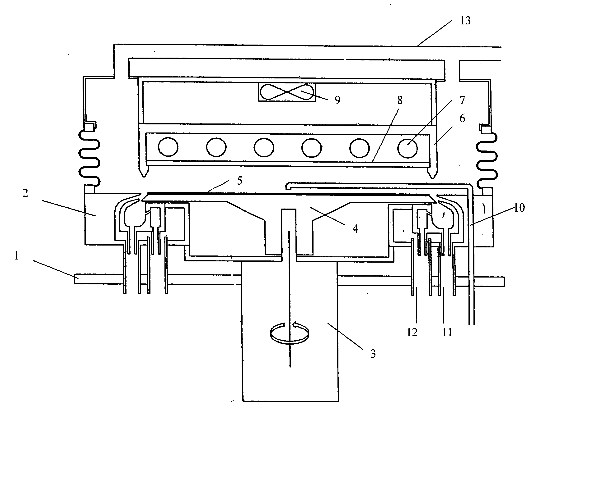
[0014] Refer to FIG. 1 which is a cross section view of a spin processor of a prior art with the heating lamps 7 raised up so that the injection pipe can go to the front side of the wafer, but do not limited on this type, any spin rinse or spin etch processor can be used equivalently. In FIG. 1, a base 1 is a fixed base for supporting the hole processor, an etching chamber 2 is a cylinder or square vacuum chamber, a wafer chuck 4 can be a vacuum chuck or a electric chuck for holding a wafer 5, the wafer chuck can be drove to spin by a motor 3, the spin speed can be adjusted from 0-3000 rpm. An etching solution injection pipe 10 is above wafer 5 for supplyin...


PUM

PropertyMeasurementUnit
Timeaaaaaaaaaa
Flow rateaaaaaaaaaa
Angular velocityaaaaaaaaaa

Abstract

The present invention discloses a puddle etching method of thin film. In a spin etching equipment, pre-wet the wafer by D.I. water and etch solution to remove the contamination and the upper layer of the film on the wafer. Then spin slowly (about 0-50 rpm) and inject etching solution to form a puddle of etching solution which will stay on the wafer, the wafer then keep spin slowly (about 0-50 rpm) such that the puddle of etching solution stay on the wafer and etching is going on by puddle etching. After the thin film is etched, the wafer is spin at higher speed, and D.I. water is injected to rinse. Then, IPA is used to remove the D.I. water by Marangoni effect. Finally raise the speed to dry the wafer.

Description

[0001] 1. Field of the Invention[0002] The present invention relates to a wet etching method of semiconductor processing, and more particularly, to a method for wet etching of thin film by forming a puddle of etching solution on the wafer in a spin processor[0003] 2. Description of Relative Prior Art[0004] In semiconductor processing, batch wet etching or spin etch by using a single wafer spin processor is usually used to etch different kinds of thin film such as silicon dioxide, silicon nitride, silicon oxynitride, poly silicon, metal film, metal-silicide film, etc. The batch method do not suitable to large diameter wafers, the single wafer spin etch is suitable to diameter above 8 inches. However, supplying etching solution to the spinning wafer will waste a lot of etching solution, the uniformity is not good enough, the reason is that the staying time of the etching solution on the center and on the periphery of the wafer is different.[0005] Using dry etching has high value of eq...

Claims


Application Information

Patent Timeline
IPC IPC(8): C23F1/08H01L21/00H01L21/311
CPCC23F1/08H01L21/67115H01L21/6708H01L21/31111
Inventor TSUNG-KUEI, KANGHO, HSIEH YUEWANG, CHIH-CHENGSHIH-YI, HSIAO
Owner GRAND PLASTIC TECH
Why Eureka
Try Eureka