Conformal thermal interface material for electronic components

a technology of thermal interface material and electronic components, which is applied in the direction of chemistry apparatus and processes, semiconductor/solid-state device details, televisions, radios, etc., can solve the problems of increasing complexity of design, increasing the size of devices, and increasing the complexity of circuit designs for modern electronic devices such as televisions, radios, etc., to facilitate the dispensing of films

Inactive Publication Date: 2003-11-06
BUNYAN MICHAEL H +1
View PDF1 Cites 46 Cited by
  • Summary
  • Abstract
  • Description
  • Claims
  • Application Information

AI Technical Summary

Benefits of technology

[0025] It therefore is a feature of the present invention to provide for the conductive cooling a heat-generating electronic component. The component has an operating temperature range above normal room temperature and a first heat transfer surface disposable in thermal adjacency with a second heat transfer surface of an associated thermal dissipation member to define an interface therebetween. A thermally-conductive material is provided which is form-stable at normal room temperature in a first phase and conformable in a second phase to substantially fill the interface. The material, which has a transition temperature from the first phase to the second phase within the operating temperature range of the electronic component, is formed into a self-supporting layer. The layer is applied to one of the heat transfer surfaces, which surfaces then are disposed in thermal adjacency to define the interface. The energization of the electronic component is effective to heat the layer to a temperature which is above the phase transition temperature.
[0027] Advantages of the present invention include a thermal interface material which melts or softens to better conform to the interfaces surfaces, but which is self-supporting and form-stable at room temperature for ease of handling and application. Further advantages include an interface material which may be formed into a film or tape without a web or other supporting substrate, and which may be applied using automated methods to, for example, the interface surface of a thermal dissipation member. Such member then may be shipped to a manufacturer for direct installation into a circuit board to thereby obviate the need for hand lay-up of the interface material. Still further advantages include a thermal interface formulation which may be tailored to provide controlled thermal and viscometric properties. These and other advantages will be readily apparent to those skilled in the art based upon the disclosure contained herein.
[0037] Although thermal dissipation member 20 is shown to be a separate heat sink member, board 14 itself may be used for such purpose by alternatively interposing interlayer 30 between surface 32 thereof and corresponding surface 34 of electronic component 12. In either arrangement, a clip, spring, or clamp or the like (not shown) additionally may be provided for applying an external force, represented at 32, of from about 1-2 lbs.sub.f for improving the interface area contact between interlayer 30 and surfaces 18 and 22 or 32 and 34.
[0040] Further in this regard, reference may be had to FIG. 2 wherein an enlarged view of a portion of interface 28 is illustrated to detail the internal morphology thereof during the energization of electronic component 12 effective to heat interlayer 30 to a temperature which is above its phase transition temperature. Interlayer 30 accordingly is shown to have been melted or otherwise softened from a form-stable solid or semi-solid phase into a flowable or otherwise conformable liquid or semi-liquid viscous phase which may exhibit relative intermolecular chain movement. Such viscous phase provides increased surface area contact with interface surfaces 18 and 22, and substantially completely fills interface 28 via the exclusion of air pockets or other voids therefrom to thereby improve both the efficiency and the rate of heat transfer through interface. Moreover, as depending on, for example, the melt flow index or viscosity of interlayer 30 and the magnitude of any applied external pressure 36 (FIG. 1), the interface gap between surfaces 18 and 22 may be narrowed to further improve the efficiency of the thermal transfer therebetween. Any latent heat associated with the phase change of the material forming interlayer 30 additionally contributes to the cooling of component 12.
[0041] Unlike the greases or waxes of such type heretofore known in the art, however, interlayer of the present invention advantageously is form-stable and self-supporting at room temperature. Accordingly, and as is shown generally at 40 in FIG. 3, interlayer 30 advantageously may be provided in a rolled, tape form to facilitate its application to the substrate by an automated process. As may be better appreciated with additional reference to FIG. 4 wherein a portion, 42, of tape 40 is shown in enhanced detail, tape 40 may be formed by applying a film of interlayer 30 to a length of face stock, liner, or other release sheet, 44. Interlayer 30 may be applied to a surface, 46, of release sheet 44 in a conventional manner, for example, by a direct process such as spraying, knife coating, roller coating, casting, drum coating, dipping, or like, or an indirect transfer process utilizing a silicon release sheet. A solvent, diluent, or other vehicle may be provided to lower the viscosity of the material forming interlayer 30. After the material has been applied, the release sheet may be dried to flash the solvent and leave an adherent, tack-free film, coating, or other residue of the material thereon.

Problems solved by technology

Circuit designs for modern electronic devices such as televisions, radios, computers, medical instruments, business machines, communications equipment, and the like have become increasingly complex.
Although the complexity of the designs has increased, the size of the devices has continued to shrink with improvements in the ability to manufacture smaller electronic components and to pack more of these components in an ever smaller area.
As electronic components have become smaller and more densely packed on integrated boards and chips, designers and manufacturers now are faced with the challenge of how to dissipate the heat which is ohmicly or otherwise generated by these components.
Indeed, it is well known that many electronic components, and especially semiconductor components such as transistors and microprocessors, are more prone to failure or malfunction at high temperatures.
Thus, the ability to dissipate heat often is a limiting factor on the performance of the component.
For high power circuits and the smaller but more densely packed circuits typical of current electronic designs, however, simple air circulation often has been found to be insufficient to adequately cool the circuit components.
However, and as is described in U.S. Pat. No. 4,869,954, the faying thermal interface surfaces of the component and heat sink typically are irregular, either on a gross or a microscopic scale.
These pockets reduce the overall surface area contact within the interface which, in turn, reduces the efficiency of the heat transfer therethrough.
Moreover, as it is well known that air is a relatively poor thermal conductor, the presence of air pockets within the interface reduces the rate of thermal transfer through the interface.
The greases and waxes of the aforementioned types heretofore known in the art, however, generally are not self-supporting or otherwise form stable at room temperature and are considered to be messy to apply to the interface surface of the heat sink or electronic component.
Moreover, use of such materials typically involves hand application or lay-up by the electronics assembler which increases manufacturing costs.

Method used


Image

  • Conformal thermal interface material for electronic components
  • Conformal thermal interface material for electronic components

Examples


Embodiment Construction

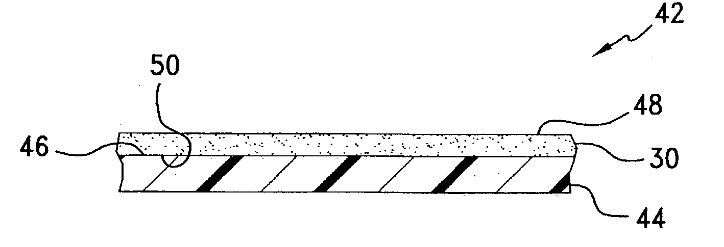
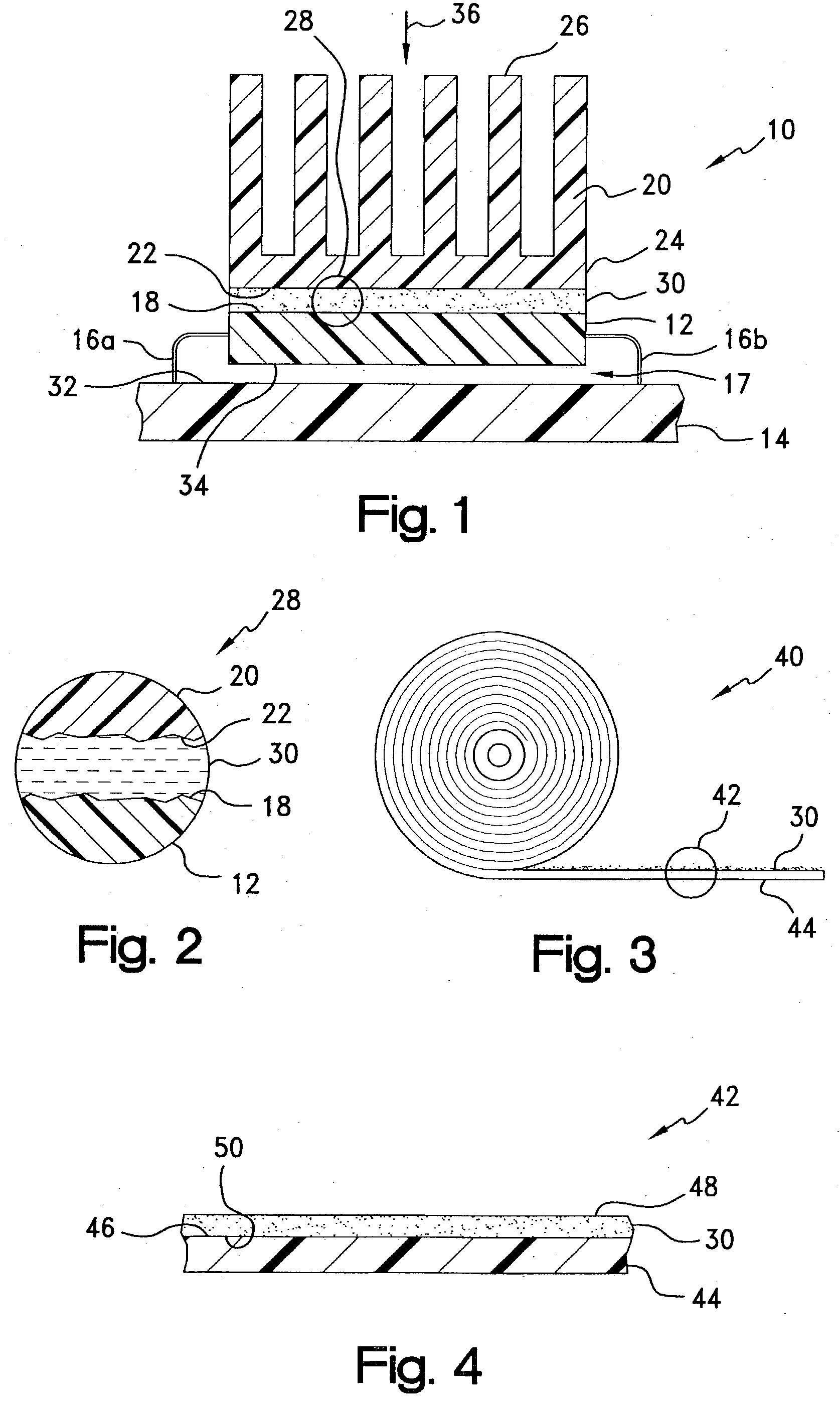
[0055] Master batches representative of the interlayer formulations of the present invention were compounded for characterization according to the following schedule:

3TABLE 3 Representative Interlayer Formulations Ultraflex .RTM. Sample Vybar .RTM. 260.sup.1 H600.sup.2 Amber.sup.3 Filler (wt. %) No. (wt. %) (wt. %) (wt. %) BN.sup.4 ZnO.sub.2.sup.5 Al.sup.6 3-1 45 2233 3-2 47 1736 3-3 47 17 6 30 3-640 60 3-7 40 19 41 3-8 50 25 25 3-10 34 16 50 5-167 33 .sup.1.alpha.-olefinic thermoplastic, Petrolite Corp., Tulsa, OK .sup.2acrylic PSA, Heartland Adhesives, Germantown, WI .sup.3paraffinic wax, Bareco Products Corp. Rock Hill, SC .sup.4Boron nitride, HCP particle grade, Advanced Ceramics, Cleveland, OH .sup.5Zinc oxide, Midwest Zinc, Chicago, II; Wittaker, Clark & Daniels, Inc., S. Plainfield, NJ .sup.6Alumina, R1298, Alcan Aluminum, Union, NJ

[0056] The Samples were thinned to about 30-70% total solids with toluene or xylene, cast, and then dried to a film thickness of from about 2.5 to...


PUM

PropertyMeasurementUnit
viscosityaaaaaaaaaa
temperatureaaaaaaaaaa
viscosityaaaaaaaaaa

Abstract

A thermally-conductive interface for conductively cooling a heat-generating electronic component having an associated thermal dissipation member such as a heat sink. The interface is formed as a self-supporting layer of a thermally-conductive material which is form-stable at normal room temperature in a first phase and substantially conformable in a second phase to the interface surfaces of the electronic component and thermal dissipation member. The material has a transition temperature from the first phase to the second phase which is within the operating temperature range of the electronic component.

Description

[0001] This application is a continuation of U.S. patent application Ser. No. 09 / 714,680, filed Nov. 16, 2000; which is an application for reissue of U.S. patent application Ser. No. 08 / 801,047, filed Feb. 14, 1997, now U.S. Pat. No. 6,054,198, granted Apr. 25, 2000, the disclosure of each of which is expressly incorporated herein by reference.[0002] The present invention relates broadly to a heat transfer material which is interposable between the thermal interfaces of a heat-generating, electronic component and a thermal dissipation member, such as a heat sink or circuit board, for the conductive cooling of the electronic component. More particularly, the invention relates to a self-supporting, form-stable film which melts or softens at a temperature or range within the operating temperature range of the electronic component to better conform to the thermal interfaces for improved heat transfer from the electronic component to the thermal dissipation member.[0003] Circuit designs ...

Claims


Application Information

Patent Timeline
Patent Type & Authority Applications(United States)
IPC IPC(8): C09K5/00C09K5/06H01L23/36H01L23/373
CPCC09K5/06H01L23/3737H01L2924/3011H01L2924/0002Y10T428/2822Y10T428/1452H01L2224/32245Y10T428/1476Y10T428/2826Y10T428/1419H01L2924/00Y10T428/31909
Inventor BUNYAN, MICHAEL H.SORGO, MIKSA DE
Owner BUNYAN MICHAEL H
Why Eureka
Try Eureka