Nitride-based semiconductor light-emitting device and manufacturing method thereof

a technology of nitride-based semiconductors and light-emitting devices, which is applied in the direction of semiconductor/solid-state device manufacturing, semiconductor devices, electrical devices, etc., can solve the problems of inability to improve light extraction efficiency, less cost of silicon substrates and large usable area, and inability to form thick nitride-based semiconductor layers

Inactive Publication Date: 2003-11-27
LEDCOMM LLC
View PDF12 Cites 137 Cited by
  • Summary
  • Abstract
  • Description
  • Claims
  • Application Information

AI Technical Summary

Problems solved by technology

In recent years, however, for the reduction of manufacturing cost of the light-emitting device, the use of silicon (Si) substrate have become common as the silicon substrate is less expensive and usable by a large area.
However, the nitride-based semiconductor layer cannot be formed thick as the difference in thermal expansion coefficient between nitride-based semiconductor layers causes crack.
Hence, it is impossible to improve light extraction efficiency by extracting light from the side surface of the nitride-based semiconductor layer using this portion to let the light emitted from the light-emitting layer pass through for the extraction.
When the film thickness of the p-type GaN semiconductor layer is increased for the formation of irregularities, many cracks are formed in the p-type GaN semiconductor layer thereby increasing the driving voltage of the device.
It is assumed that when the p-type GaN semiconductor layer is grown at a high temperature and brought back to room temperature after the growth, tensile stress applied on the p-type GaN s

Method used


Image

  • Nitride-based semiconductor light-emitting device and manufacturing method thereof
  • Nitride-based semiconductor light-emitting device and manufacturing method thereof
  • Nitride-based semiconductor light-emitting device and manufacturing method thereof

Examples


first embodiment

[0065] (First Embodiment)

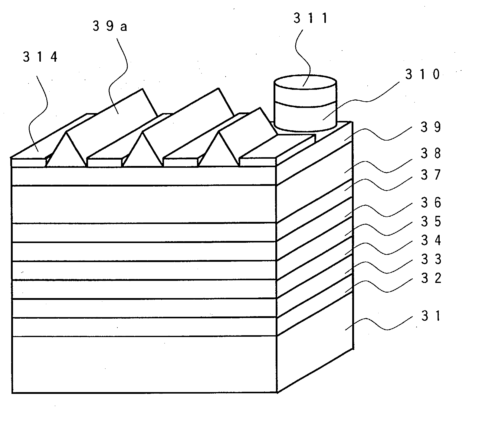
[0066] FIG. 1 shows a schematic perspective of the nitride-based semiconductor light-emitting device of the first embodiment of the present invention. The nitride-based semiconductor light-emitting device of the embodiment includes on a support substrate 11 of Ni plating functioning also as an electrode, a p-type-use electrode 12, and further a p-type GaN clad layer 13, a p-type AlGaInN carrier block layer 14, a light-emitting layer 15 of In.sub.xGa.sub.1-xN, an Si-doped n-type In.sub.0.03Ga.sub.0.97N clad layer 16, an Si-doped n-type In.sub.0.1Ga.sub.0.9N layer 17 and an Si-doped n-type GaN layer clad layer 18 successively formed on p-type-use electrode 12. Further, an n-type GaN light extracting layer 19 having irregularities formed through regrowth is formed on an upper surface of n-type GaN clad layer 18 and an n-type-use electrode 110 and an n-type-use bonding electrode 111 are formed in a portion of n-type GaN light extracting layer 19.

[0067] In the fo...

second embodiment

[0082] (Second Embodiment)

[0083] FIG. 4 shows a schematic perspective of a nitride-based semiconductor light-emitting device of the second embodiment of the present invention. The nitride-based semiconductor light-emitting device of the embodiment is characterized in that an Al translucent electrode layer 213 is formed through vapor deposition on an upper surface of n-type GaN light extracting layer 29 having irregularities.

[0084] The nitride-based semiconductor light-emitting device of the embodiment includes on a support substrate 21 of Ni plating functioning also as an electrode, a p-type-use electrode 22, and further a p-type GaN clad layer 23, a p-type AlGaInN carrier block layer 24, an In.sub.xGa.sub.1-xN light-emitting layer 25, an Si-doped n-type In.sub.0.03Ga.sub.0.97N clad layer 26, an Si-doped n-type In.sub.0.1Ga.sub.0.9N layer 27 and an Si-doped n-type GaN layer clad layer 28 successively formed on p-type-use electrode 22. Further on n-type GaN clad layer 28, an n-type G...

third embodiment

[0086] (Third Embodiment)

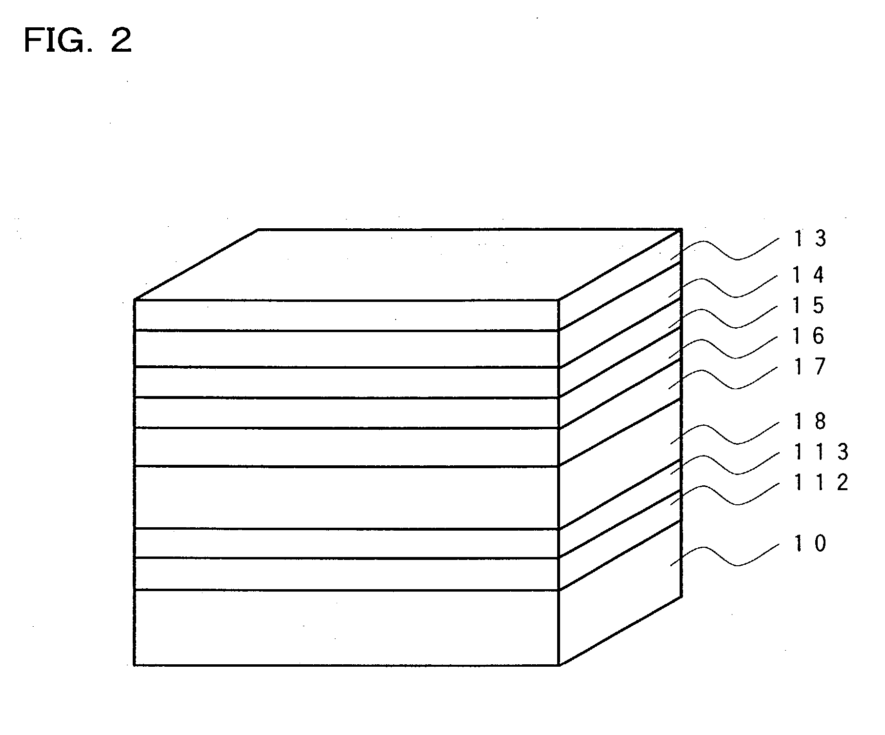
[0087] FIG. 5 shows a schematic perspective of a nitride-based semiconductor light-emitting device of the third embodiment of the present invention. The nitride-based semiconductor light-emitting device of the embodiment is characterized in that an SiO.sub.2 mask 314 is formed above an upper surface of Si-doped n-type GaN layer clad layer 38 and that a pyramid-shaped light extracting surface 39a is formed in an n-type GaN light extracting layer 39 which is selectively grown.

[0088] The nitride-based semiconductor light-emitting device of the embodiment includes on a support substrate 31 of Ni plating functioning also as an electrode, a p-type-use electrode 32, and further, a p-type GaN clad layer 33, a p-type AlGaInN carrier block layer 34, an In.sub.xGa.sub.1-xN light-emitting layer 35, an Si-doped n-type In.sub.0.03Ga.sub.0.97N clad layer 36, an Si-doped n-type In.sub.0.1Ga.sub.0.9N layer 37 and an Si-doped n-type GaN layer clad layer 38 successively formed...


PUM


Abstract

The nitride-based semiconductor light-emitting device and manufacturing method thereof are disclosed: the nitride-based semiconductor light-emitting device includes a reflective layer formed on a support substrate, a p-type nitride-based semiconductor layer, a light-emitting layer and an n-type nitride-based semiconductor layer successively formed on the reflective layer, wherein irregularities are formed on a light extracting surface located above the n-type nitride-based semiconductor layer.

Description

[0001] 1. Field of the Invention[0002] The present invention relates to a nitride-based semiconductor light-emitting device using a nitride-based semiconductor represented by the general formula In.sub.xAl.sub.yGa.sub.1-x-yN (x+y+z=1, 0.ltoreq.x.ltoreq.1, 0.ltoreq.y.ltoreq.1 and 0.ltoreq.z.ltoreq.1) and a manufacturing method thereof.[0003] 2. Description of the Background Art[0004] The conventional nitride-based semiconductor light-emitting devices are mostly fabricated by layering a nitride-based semiconductor layer on a sapphire substrate. In recent years, however, for the reduction of manufacturing cost of the light-emitting device, the use of silicon (Si) substrate have become common as the silicon substrate is less expensive and usable by a large area.[0005] FIG. 12 shows a schematic perspective of a conventional nitride-based semiconductor light-emitting device using an Si substrate. The nitride-based semiconductor light-emitting device includes on an Si substrate 100, an AlN...

Claims


Application Information

Patent Timeline
IPC IPC(8): H01L33/06H01L21/205H01L33/10H01L33/16H01L33/22H01L33/32H01L33/34H01L33/40
CPCH01L33/22H01L33/42H01L33/38
Inventor KOIDE, NORIKATSUHATA, TOSHIOFUDETA, MAYUKOKIMURA, DAIGAKU
Owner LEDCOMM LLC
Why Eureka
Try Eureka