This helps you quickly interpret patents by identifying the three key elements:
Problems solved by technology
Method used
Benefits of technology
Benefits of technology
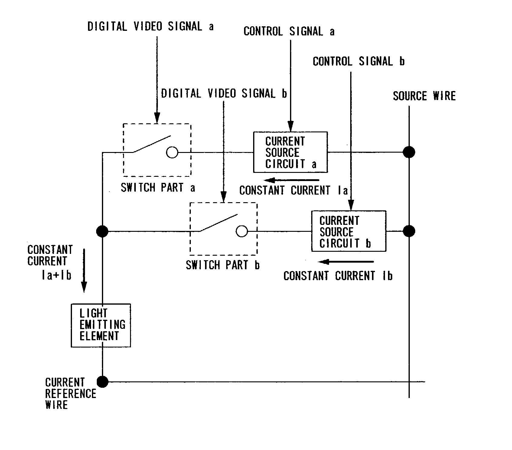
[0048] As to each of a plurality of the switch parts, on or off thereof is selected by a digital video signal. When the switch part is turned on(conductive), a current flows from the current source circuit which corresponds to the switch part to the light emitting element so that the light emitting element emits lights. A current which is supplied from one current source circuit to the light emitting element is constant. According to the current rule of Kirchhoff, a value of a current which flows through the light emitting element is comparable to an added value of currents which are supplied from all current source circuits corresponding to the switch part of a conductive state to the light emitting element. In the pixel of the invention, the value of the current which flows through the light emitting element is changed by which switch part out of a plurality of the switch parts is turned conductive so that it is possible to express gradation. On one hand, the current source circuit is set to always output a constant current of a certain level. On that account, it is possible to prevent variation of the current which flows through the light emitting element.
[0051] The current source circuit (current source circuit a, current source circuit b) has an input terminal and an output terminal, and has a function for having a constant current flowed between the input terminal and the output terminal. The current source circuit a is controlled to have the constant current Ia flowed by a control signal a. Also, the current source circuit b is controlled to have the constant current Ib flowed by a control signal b. The control signal may be a signal which is different from the video signal. Also, the control signal may be a current signal or may be a voltage signal. In this manner, an operation for determining a current which flows through the current source circuit by the control signal is called as a setting operation of the current source circuit or a setting operation of the pixel. Timing of carrying out the setting operation of the current source circuit may be synchronous with or may be asynchronous with the operation of the switch part, and can be set at arbitrary timing. Also, the setting operation may be carried out only to one current source circuit and information of the current source circuit to which the setting operation was carried out may be shared with other current source circuit. By the setting operation of the current source circuit, it is possible to suppress variation of a current which the current source circuit outputs.
[0065] Then, an effective technique for further reducing the luminance variation in the above-described gradation display technique will be shown. This is an effective technique in case that the luminance is varied due to for example, noise etc. even when the same gradation is expressed between the pixels.
[0066] Each of more than two current source circuits out of a plurality of current source circuits that each pixel has is set so as to output the same constant current each other. And, on the occasion of expressing the same gradation, the current source circuits which output the same constant current are selectively used. If this is realized, even if the output current of the current source circuit is fluctuated, the current flowing through the light emitting element is temporarily averaged. On that account, it is possible to visually reduce the variation of the luminance due to the variation of the output currents of the current source circuits between respective pixels.
[0067] In the invention, since the current flowing through the light emitting element on the occasion of carrying out image display is maintained at a predetermined constant current, regardless of change of the current characteristic due to deterioration etc., it is possible to have the light emitting element emitted light with constant luminance. Since on or off state of the switch part is selected by the digital video signal and thereby, the light emitting state or the non light emitting state of each pixel is selected, it is possible to quicken the writing of the video signal to the pixel. In the pixel in which the non light emitting state was selected by the video signal, since the current to be inputted to the light emitting element is completely blocked by the switch part, it is possible to express accurate gradation. In short, it is possible to solve the problem of contrast deterioration on the occasion of black display which occurs due to the leak current. Also, in the invention, since it is possible to set the current value of the constant current flowing through the current source circuit large on some level, it is possible to reduce the influence of noise which occurs on the occasion of writing a small signal current. Further, since the display device of the invention does not need a drive circuit for changing the value of the current flowing through the current source circuit which was placed in each pixel and there is no necessity of an external drive circuit which was fabricated on a separate substrate such as a single crystalline IC substrate etc., it is possible to realize a lower cost and a smaller size.
Problems solved by technology
In short, in the voltage writing type analog system, when the current characteristic of the drive TFT 3004 varies, the drain current varies and therefore, there is a problem that luminance of the EL element 3306 varies between pixels.
As a result, in a display device having a pixel of such a type that the drive TFT is made to be operated in the linear region, burn-in of an image tends to occur.
On that account, it is difficult to quickly write the signal current.
On that account, there is such a high risk that it is impossible to have the pixel emitted light with accurate luminance.
However, in reality, it is hard to have completely the same current characteristics of the pair of these TFTs, and there occurs variation.
Even in case that the black display is carried out, there is such a possibility that the drain current flows through the drive TFT 2903 and the EL element 2906 emits light, and there occurs a problem that contrast comes down.
However, in a transistor which used polycrystalline semiconductors etc., since variation of characteristics of transistors is large, it is difficult to make the video signal input current source in which current characteristics are uniform.
The display device of such structure has such problems that cost is high, and an area of a picture frame can not be reduced since large is an area which is required on the occasion of attachment of the single crystalline IC substrate.
However, only by the above-described method, there is a case that the number of gradation is few.
Method used
Image
Click on the blue label to locate the original text in one second.
Reading with bidirectional positioning of images and text.
Examples
embodiment 1
[0112] (Embodiment 1)
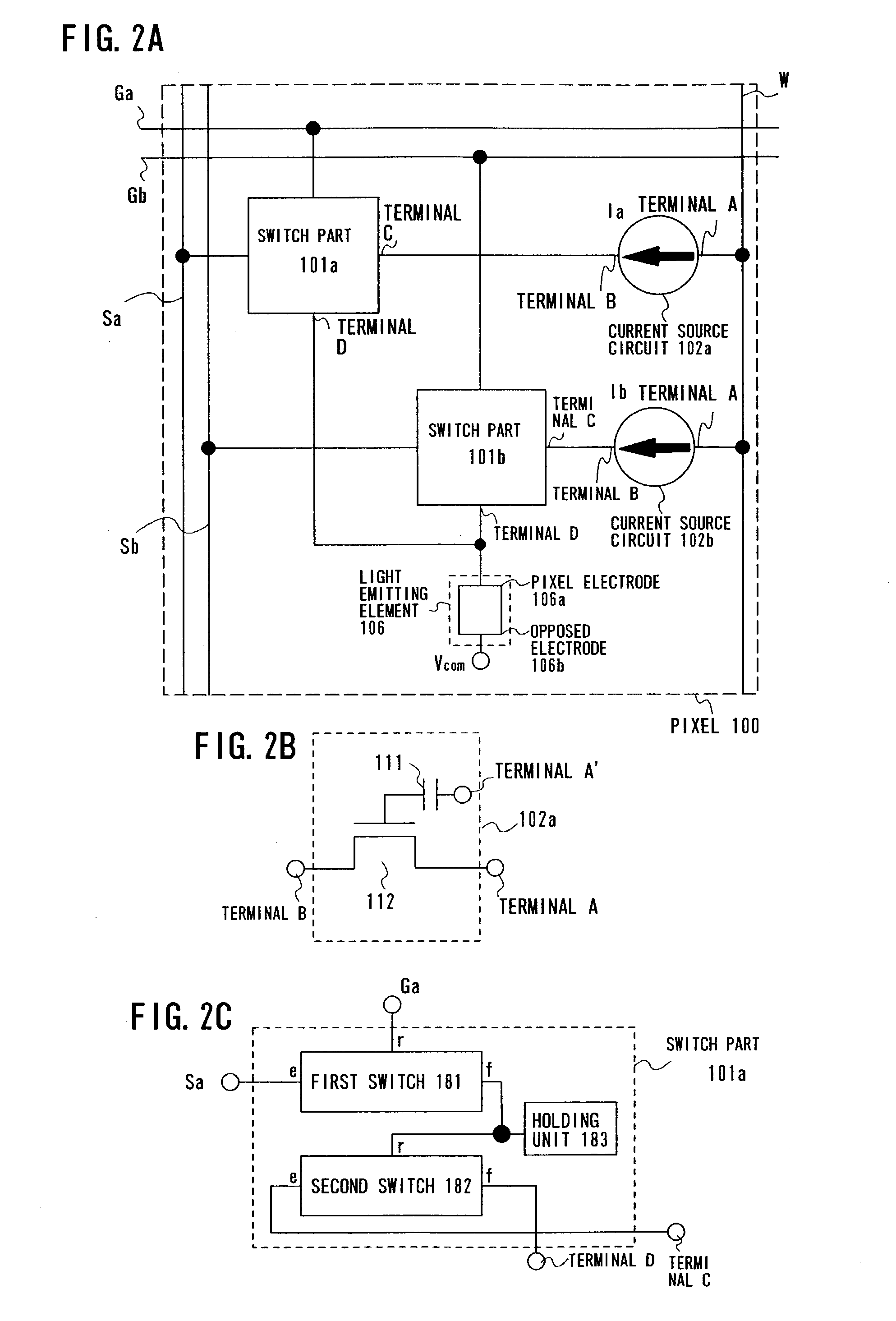
[0113] An embodiment of the invention will be described by use of FIG. 2. In this embodiment, a case that there are two pairs in one pixel will be described.
[0114] In FIG. 2A, each pixel 100 has switch parts 101a and 101b, current source circuits 102a and 102b, a light emitting element 106, video signal input lines Sa and Sb, scanning lines Ga and Gb, and a power supply line W. The switch part 101a and the current source circuit 102a are connected serially to form one pair. The switch part 102b and the current source circuit 102b are connected serially to form one pair. These two pairs are connected in parallel. Also, these two parallel circuits are serially connected to the light emitting element 106.
[0115] In the pixel shown in FIG. 2, two pairs are disposed but, hereinafter, paying attention to the pair of the switch part 101a and the current source circuit 102a, a structure of the current source circuit 102a and the switch part 101a will be described by use ...
embodiment 2
[0136] (Embodiment 2)
[0137] This embodiment shows a concrete structural example of the switch part of each plural pairs of a switch part and a current source circuit that the pixel has in the display device of the invention. Also, an operation of the pixel which has the switch part will be described.
[0138] A structural example of the switch part is shown in FIG. 3. A switch part 101 has a selection transistor 301, a drive transistor 302, a deletion transistor 304, and a holding capacitance 303. In addition, it is possible to omit the holding capacitance 303 by using a gate capacitance etc. of the drive transistor 302. A transistor which configures the switch part 101 may be a single crystalline transistor, or a polycrystalline transistor, or an amorphous transistor. Also, it may be a SOI transistor. It may be a bipolar transistor. It may be a transistor which used an organic material, for example, a carbon nanotube.
[0139] A gate electrode of the selection transistor 301 is connected...
embodiment 3
[0168] (Embodiment 3)
[0169] In this embodiment, a structure and an operation of the current source circuit that each pixel of the display device of the invention has will be described in detail.
[0170] The current source circuit of one pair out of a plurality of pairs of a switch part and a current source circuit that each pixel has will be noted, and a structure thereof will be described in detail. In this embodiment, five structural examples of the current source circuit will be cited but, another structural example may be fine if it is a circuit which operates as a current source. In addition, a transistor which configures the current source circuit may be a single crystalline transistor, or a polycrystalline transistor, or an amorphous transistor. Also, it may be a SOI transistor. It may be a bi-polar transistor. It may be a transistor which used an organic material, for example, a carbon nanotube.
[0171] Firstly, a current source circuit of a first structure will be described by ...
PUM
Abstract
To provide a display device capable of allowing a light emitting element to emit light with a constant luminance while being free of an influence of deterioration over time and capable of accurate gradation display and high-speed writing of signal current to each pixel as well, in which an influence of noise causing leak current etc. is suppressed, and a driving method therefor. According to the present invention, plural pairs of switch portion and current source circuit are provided. Each of the plural switch portions is controlled in its switching operation according to a digital videosignal. When the switch portion turns on, the current source circuit corresponding to the switch portion supplies current to allow the light emitting element to emit light. The current supplied from one current source circuit to the light emitting element is constant and a value of current flowing into the light emitting element corresponds to the total value of currents supplied to the respective light emitting elements from all the current source circuits corresponding to the switch portions in a conductive state.
Description
BACKGROND OF THE INVENTION[0001] 1. Field of the Invention[0002] The present invention relates to a display device in which a light emitting element is used and a driving method therefor. More specifically, the present invention relates to an active matrixdisplay device in which the light emitting elements are arranged for each pixel and a transistor for controlling light emission of the light emitting elements is formed, and to a driving method therefor.[0003] 2. Description of the Related Art[0004] Development of a display device having a light emitting element has been put forward in these years. In particular, development of an active matrix type display device in which a light emitting element and a transistor for controlling light emission of the light emitting element are disposed with respect to each pixel has been put forward.[0005] In the active matrix type display device, either a technique in which an input of luminance information to each pixel is carried out by a volt...
Claims
Application Information
Patent Timeline
Application Date:The date an application was filed.
Publication Date:The date a patent or application was officially published.
First Publication Date:The earliest publication date of a patent with the same application number.
Issue Date:Publication date of the patent grant document.
PCT Entry Date:The Entry date of PCT National Phase.
Estimated Expiry Date:The statutory expiry date of a patent right according to the Patent Law, and it is the longest term of protection that the patent right can achieve without the termination of the patent right due to other reasons(Term extension factor has been taken into account ).
Invalid Date:Actual expiry date is based on effective date or publication date of legal transaction data of invalid patent.

