Thin film semiconductor device and manufacturing method

a technology of thin film and manufacturing method, applied in the direction of power consumption reduction, pulse technique, instruments, etc., can solve the problems of reduced circuit operation speed, increased power dissipation, and reduced power consumption of low-energy devices

Active Publication Date: 2004-03-11
HANNSTAR DISPLAY CORPORATION
View PDF14 Cites 34 Cited by
  • Summary
  • Abstract
  • Description
  • Claims
  • Application Information

AI Technical Summary

Benefits of technology

[0014] Accordingly, it is an object of the present invention to provide a thin film semiconductor device and its manufacturing method for forming n-channel TFTs and p-channel TFTs, both of which have a VT suitable for each circuit, without making manufacturing process complicated and for increasing the performance of an analog circuit without increasing power dissipation.
[0026] The thin film semiconductor device according to the present invention has the configuration described above in which, on a polycrystalline silicon film formed on an insulating substrate such as a glass, high-VT TFTs are formed so that the off current of a logic circuit or a switch is reduced, and low-VT TFTs are formed so that the operation speed and the dynamic range of an analog circuit are increased, without making the fabrication process complicated. Because the same dopant at an approximately equal density is added to n-channel TFTs and p-channel TFTs for which channel doping is performed, VT symmetry can be maintained and therefore TFTs suitable for each circuit can be built.
[0031] The effect of the present invention is that TFTs each with a different VT may be formed for each of n-channel TFTs and p-channel TFTs without increasing the number of processes.
[0033] Another effect of the present invention is that VT symmetry between n-channel TFTs and p-channel TFTs is maintained and therefore the circuit can be designed optimally.
[0035] The further effect of the present invention is that a circuit including logics or switches that have good off-characteristics and analog circuits that have high operation speeds and wide dynamic rages may be formed easily.

Problems solved by technology

An off-leakage current, if large, power dissipation is increased because a leakage current flows even when the circuit is inactive.
This is a serious problem especially for driver circuits in a mobile device where the battery life is one of important performance factors.
In addition, a recent demand for low energy requires even non-mobile devices to reduce power dissipation during operation time and to reduce standby power dissipation during standby time.
This generates other problems such as a reduced operation speed of a circuit or a narrower dynamic range (output voltage range against to power voltage range) of an analog circuit.

Method used


Image

  • Thin film semiconductor device and manufacturing method
  • Thin film semiconductor device and manufacturing method
  • Thin film semiconductor device and manufacturing method

Examples


first embodiment

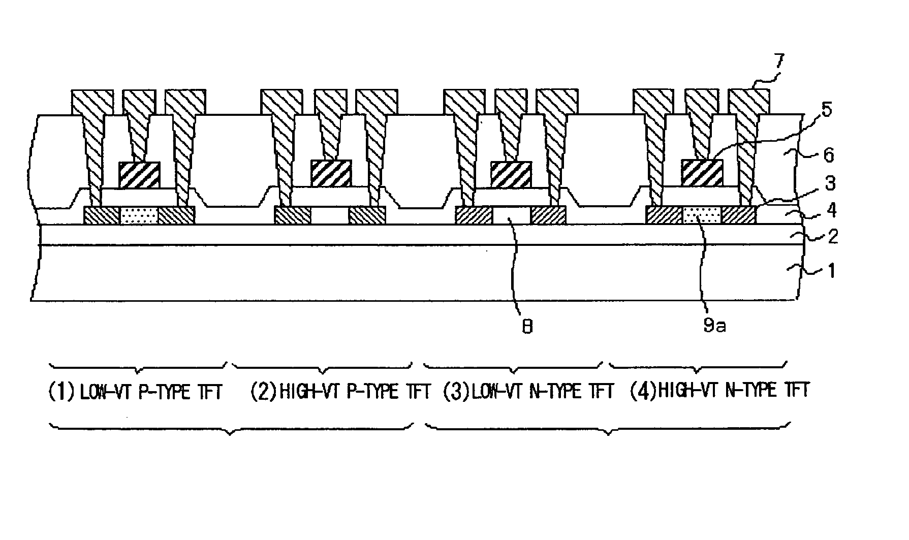
[0088] First, an analog circuit comprising TFTs, which have two kinds of VTs, according to the present invention will be described with reference to FIG. 8. FIG. 8 is a circuit diagram showing an example in which the configuration according to the present invention is applied to a differential amplifier circuit. In the description below, it is assumed that both high-VT TFTs and low-VT TFTs are insulated gate type transistors.

[0089] As shown in FIG. 8, the circuit according to the present embodiment is a differential amplifier circuit comprised of the differential stage and the amplifier stage wherein low-VT TFTs are used in the differential stage (23 in FIG. 8). In the differential amplifier circuit, the differential pair transistors 101 and 102 are composed by low-VT TFTs and a switch 501 for controlling to off current path to the differential pair 101 and 102 is composed by a high-VT TFT. All the components other than the differential pair 101 and 102 are composed by a high-VT TFT...

second embodiment

[0094] Next, an analog circuit comprising TFTs, having two kinds of VTs, in accordance with the present invention will be described with reference to FIG. 9. FIG. 9 shows a differential amplifier circuit in which low-VT TFTs are used in the differential stage (23 in FIG. 9). That is, in this differential amplifier circuit, a differential pair comprised of transistors 101 and 102 and a current mirror circuit comprised of transistors 103 and 104 are formed by low-VT TFTs, and a switch 501 for cutting off a current path to the differential pair and the current mirror circuit is formed by a high-VT TFT. All the components other than the differential pair comprised of transistors 101 and 102 and the current mirror circuit comprised of transistors 103 and 104 are formed by a high-VT TFT similar to that used for the switch 501.

[0095] The differential pair transistors 101 and 102, composed of low-VT TFTs, extend the operation range of the differential stage 23 as in FIG. 8 and hence the dyn...

third embodiment

[0096] Next, an analog circuit comprising TFTs, having two kinds of VTs, in accordance with the present invention will be described with reference to FIG. 10. FIG. 10 is a circuit diagram showing another example in which the structure of the present invention is applied to a differential amplifier circuit.

[0097] As shown in FIG. 10, the circuit in the present embodiment is a differential amplifier circuit in which low-VT TFTs are used in the differential stage (23 in FIG. 10) and the amplifier stage (24 in FIG. 10). That is, in this differential amplifier circuit, a differential pair (101 and 102) and a current mirror circuit (103 and 104) are formed by low-VT TFTs, a switch 501 for cutting off a current path to the differential pair and the current mirror circuit is formed by a high-VT TFT, a p-channel transistor 106 in the amplifier stage is formed by a low-VT TFT, and a switch 504 for cutting off a current path between a high potential power supply terminal 13 and an output termi...


PUM

PropertyMeasurementUnit
thicknessaaaaaaaaaa
insulatingaaaaaaaaaa
threshold voltagesaaaaaaaaaa

Abstract

When n-channel thin film transistors(TFTs) and p-channel TFTs are formed on a polycrystalline silicon film formed on a glass substrate, a process is included in which P-dopant or N-dopant is introduced at the same time to the channel region of a part of the n-channel TFTs and a part of the p-channel TFTs. In one channel doping operation, a set of low-VT and high-VT p-channel TFTs and a set of low-VT and high-VT n-channel TFTs can be formed. This method is used for forming high-VT TFTs, which can reduce the off-current, in logics and switch circuits and for forming low-VT TFTs, which can enlarge the dynamic range, in analog circuits to improve the performance of a thin film semiconductor.

Description

[0001] The present invention relates to a thin film semiconductor device and a method of manufacturing the thin film semiconductor device, and more particularly to a thin film semiconductor device, which includes at least an analog circuit part and a switch using thin film transistors (TFT: an abbreviation of a thin film transistor) having different threshold voltages (a threshold voltage is also designated as VT in the below), and a manufacturing method thereof.[0002] A display device, such as a liquid crystal display device and an organic EL (electroluminescence) display device that are thinner and lighter than a CRT, has been used as the monitor of a portable terminal such as a cellular phone and a mobile device or as the monitor of a notebook personal computer. An image is displayed on a liquid crystal display device or an organic EL display device by forming a display part, which has pixels arranged in a matrix, on an insulating substrate such as a glass substrate using the thi...

Claims


Application Information

Patent Timeline
Patent Type & Authority Applications(United States)
IPC IPC(8): G02F1/1368G11C7/06H01L21/77H01L21/84H01L27/12H01L29/786H03F3/45H03K5/24H03K19/00
CPCG11C7/062H01L27/1214H03K19/0016H03F3/45219H03K5/2481H03F3/45192H01L27/1218H01L27/127
Inventor SERA, KENJITSUCHI, HIROSHI
Owner HANNSTAR DISPLAY CORPORATION
Why Eureka
Try Eureka