

Rapidly testable semiconductor memory device
- Summary
- Abstract
- Description
- Claims
- Application Information
AI Technical Summary
Benefits of technology
Problems solved by technology
Method used
Image

Examples
first embodiment
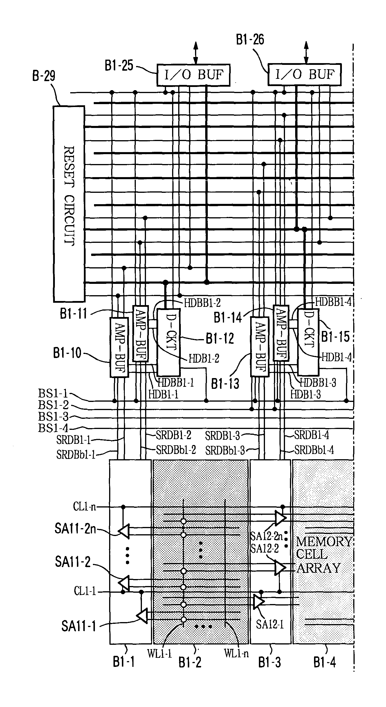
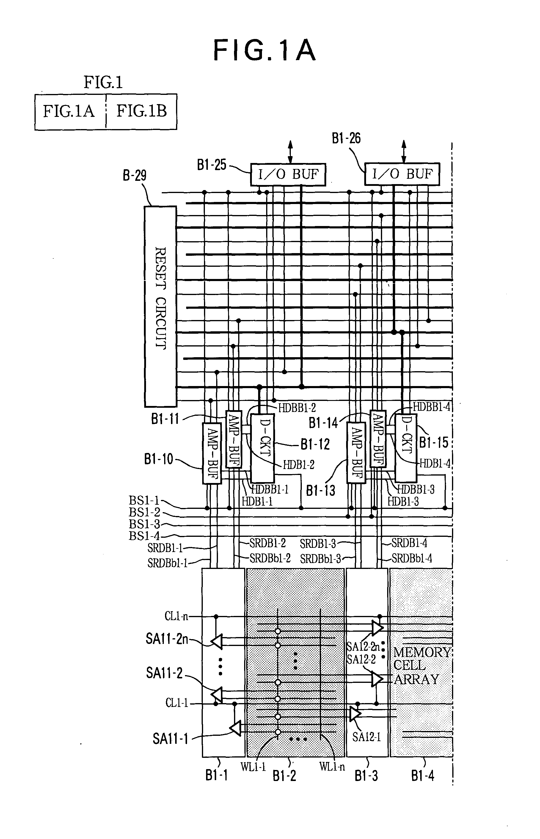
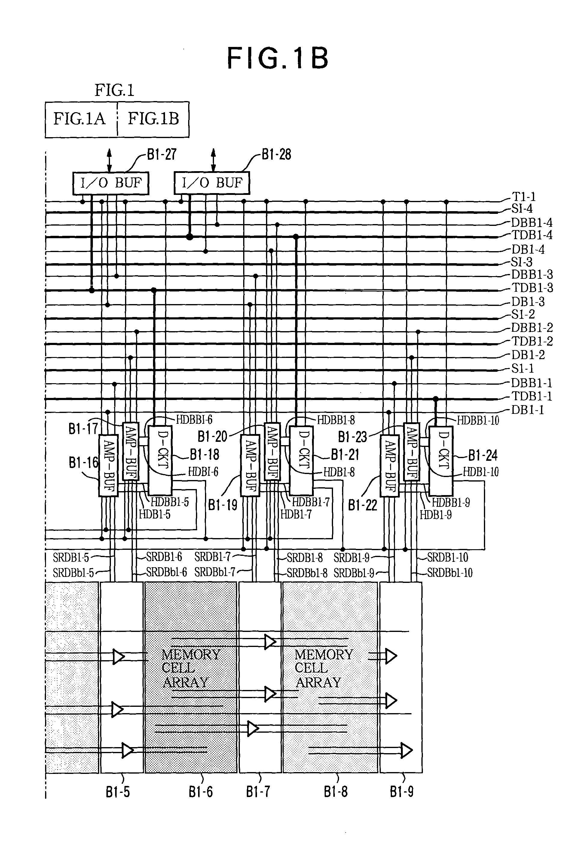
[0041] Referring to FIGS. 1A and 1B, the invention is a semiconductor memory device comprising four memory cell arrays B1-2, B1-4, B1-6, B1-8 interspersed among five sense amplifier arrays B1-1, B1-3, B1-5, B1-7, B1-9. The memory cell arrays are spanned by n column lines CL1-1 to CL1-n, where n is an integer greater than one. Each column line activates four sense amplifiers adjacent each memory cell array: for example, the first column line CL1-1 activates sense amplifiers SA11-1 and SA11-2 in the sense amplifier array B1-1 on one side of memory cell array B1-2 and sense amplifiers SA12-1 and SA12-2 in the sense amplifier array B1-3 on the other side of memory cell array B1-2. Each sense amplifier is coupled to a complementary pair of bit lines extending across the adjacent memory cell array or arrays. Each memory cell array includes n word lines WL1-1 to WL1-n, and n.times.n memory cells, indicated by white circles, disposed at alternate intersections of the word lines and the comp...
second embodiment
[0089] Referring to FIGS. 13A, 13B, and 13C, the second embodiment is generally similar to the first embodiment but has twice as many memory cell arrays, and tests twice as many bits at once. Specifically, the second embodiment has eight memory cell arrays B3-2, B3-4, B3-6, B3-8, B3-10, B3-12, B3-14, B3-16 interspersed among nine sense amplifier arrays B3-1, B3-3, B3-5, B3-7, B3-9, B3-11, B3-13, B3-15, B3-17. The sense amplifier arrays are connected by complementary pairs of read data bus lines SRDB3-1, SRDBb3-1, . . . , SRDB3-18, SRDBb3-18 to output amplifier-input buffers B3-18, B3-19, B3-21, B3-22, B3-24, B3-25, B3-27, B3-28, B3-30, B3-31, B3-33, B3-34, B3-36, B3-37, B3-39, B3-40, B3-42, B3-43 which provide amplified read data to primary decision circuits B3-20, B3-23, B3-26, B3-29, B3-32, B3-35, B3-38, B3-41, B3-44 via comparison data buses HDB3-1, HDBB3-1, . . . , HDB3-18, HDBB3-18, as described in the first embodiment.
[0090] The comparison results obtained by each adjacent pai...
third embodiment
[0104] Referring to FIGS. 16A, 16B, and 16C, the third embodiment comprises the same sense amplifier arrays, memory cell arrays, output amplifier-input buffers, primary and secondary decision circuits, input-output buffers, reset circuit, data bus lines, read data bus lines, comparison data bus lines, test data bus lines, shield lines, and block select signal lines as the second embodiment. These elements are indicated by the same reference characters as in the second embodiment, except that `B3` and `S3` are changed to `B4` and `S4`: for example, the first sense amplifier array is now designated B4-1, and the first block select signal line is now designated BS4-1.
[0105] The third embodiment differs from the second embodiment in having two test control signal lines T4-1 and T4-2. Both test control signal lines are connected to the output amplifier-input buffers B4-18 etc., primary decision circuits B4-20 etc., reset circuit B4-53, and input-output buffers B4-54 to B4-57. The second ...
PUM
 Abstract
Description
Claims
Application Information