

Memory module and memory system
a memory module and memory technology, applied in the field of memory modules and memory systems, can solve the problems of inability to increase memory capacity, inability to increase memory, and increase the degradation of signal waveforms, so as to increase the signal transmission speed, reduce the pass of signals through connectors, and achieve high-capacity memory
- Summary
- Abstract
- Description
- Claims
- Application Information
AI Technical Summary
Benefits of technology
Problems solved by technology
Method used
Image

Examples
first embodiment
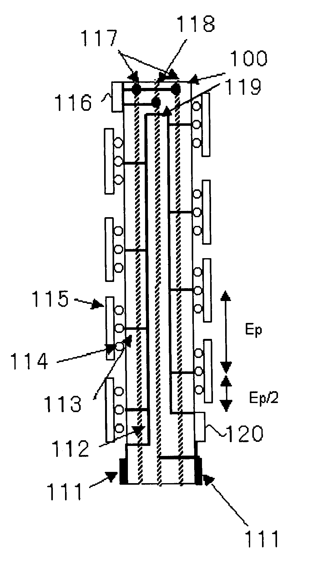
[0075] FIGS. 1A and 1B is a diagram showing an example of the configuration of a memory module in accordance with the present invention. FIG. 1A is a cross sectional view and FIG. 1B is a top view wherein one DQ bus line is shown. Referring to FIGS. 1A and 1b, a memory module in accordance with the present embodiment has a plurality of DRAMs 115, which share a bus line, on the front surface and the back surface of the module board. The bus line is extended on the front surface of the board from a first module terminal (DQ) 111 to a via hole 113 spaced from the first module terminal and is connected to one end of a first strip line 112 through the via hole 113. The signal terminal of a DRAM 115 mounted on the front surface of the board is connected to the first strip line 112 through an associated via hole. The first strip line is extended in one direction, and the other end corresponding to said one end is connected to the one end of a second strip line 112 on the back surface throu...
second embodiment
[0129] FIGS. 6A and 6B are diagrams showing the configuration of a memory module in the present invention. As shown in FIG. 6A, the memory module may also be composed by a multi-chip module 61 using a memory with a built-in termination 115.
[0130] The memory module has an MCM (Multi-Chip Module) board 61 on which a plurality of memory devices 115, which share a data bus line, are mounted on the front surface and the back surface. The bus line is connected to one end of a strip line through a via hole 113. The terminals of the plurality of DRAMs 115 mounted on the front surface and the back surface of the board are connected alternately to the strip line 112 through via holes. The other end of the strip line 112 is connected to the termination circuit included DRAM 115 through a via hole and is terminated.
[0131] This configuration makes the memory module compact. It is also possible that the memory devices (chips) 115 on the top and back surfaces may be wired alternately. Such a confi...
third embodiment
[0133] Next, a memory module in accordance with the present invention will be described. As shown in FIG. 7, a plurality of memories may be composed by a multi-chip packages 70A and 70B. The multi-chip packages 70A and 70B each have the memory module configuration as shown in FIG. 6. The multi-chip package 70A connected to a printed circuit board 701 has DRAMs 115 mounted on an insulating board 710. The multi-chip package 70A is connected to the printed circuit board 701 via a pin 711 and is connected to a pin of the multi-chip package 70B on the back surface via a through hole (via hole) 702 provided through the printed circuit board 701. The strip line of the multi-chip package 70B is connected to the pattern on the board through the pin 711 and is connected to a termination resistor 704. This configuration reduces the size of a large-capacity memory module and makes the system size more compact. Especially, the configuration reduces the height, making the module a low-profile mod...
PUM
 Abstract
Description
Claims
Application Information