Method and apparatus for optical film measurements in a controlled environment

a controlled environment and optical film technology, applied in the direction of manufacturing tools, lapping machines, instruments, etc., can solve the problems of significant cost, significant delay between the polishing operation and the measurement of the results of the polishing operation, and it is not practicable to measure the film thickness immediately after the polishing process

Inactive Publication Date: 2004-06-10
TAIWAN SEMICON MFG CO LTD
View PDF2 Cites 9 Cited by
  • Summary
  • Abstract
  • Description
  • Claims
  • Application Information

AI Technical Summary

Benefits of technology

[0014] This embodiment of the probe includes a high pressure vortex air jet that rapidly clears both the surface containing the films to be measured and the window of the probe itself, thus enabling the passage of a measurement beam through air to the surface being tested.
[0016] In addition to improving the feedback control loop characteristics, measurements performed in accordance with the invention have been shown to improve polish cycle time by at least 25%.
[0018] Exemplary embodiments of the invention do not require handling and significantly reduce the cost of conventional systems. Additionally, exemplary embodiments of the invention are inexpensive to implement and may take advantage of existing part handling equipment. For example, the wafer is already chucked in the polishing tool and the wafer does not need to be removed from this chuck for exemplary embodiments of this invention.

Problems solved by technology

Thus, there is a significant delay between the polishing operation and the measurement of the results of the polishing operation.
There is also excessive handling of the wafers between the polishing tool and the measurement area which results in significant cost.
However, this has not been practical to measure the film thickness immediately after the polishing process, because the wafer is placed in a rinsing tank and rinsed with water.
It is very difficult to obtain an accurate thin film measurement in this environment.
Additionally, since the wafers are wet and in a moist environment, but not totally immersed all of the time, the environment is non-uniform.

Method used


Image

  • Method and apparatus for optical film measurements in a controlled environment
  • Method and apparatus for optical film measurements in a controlled environment
  • Method and apparatus for optical film measurements in a controlled environment

Examples


Embodiment Construction

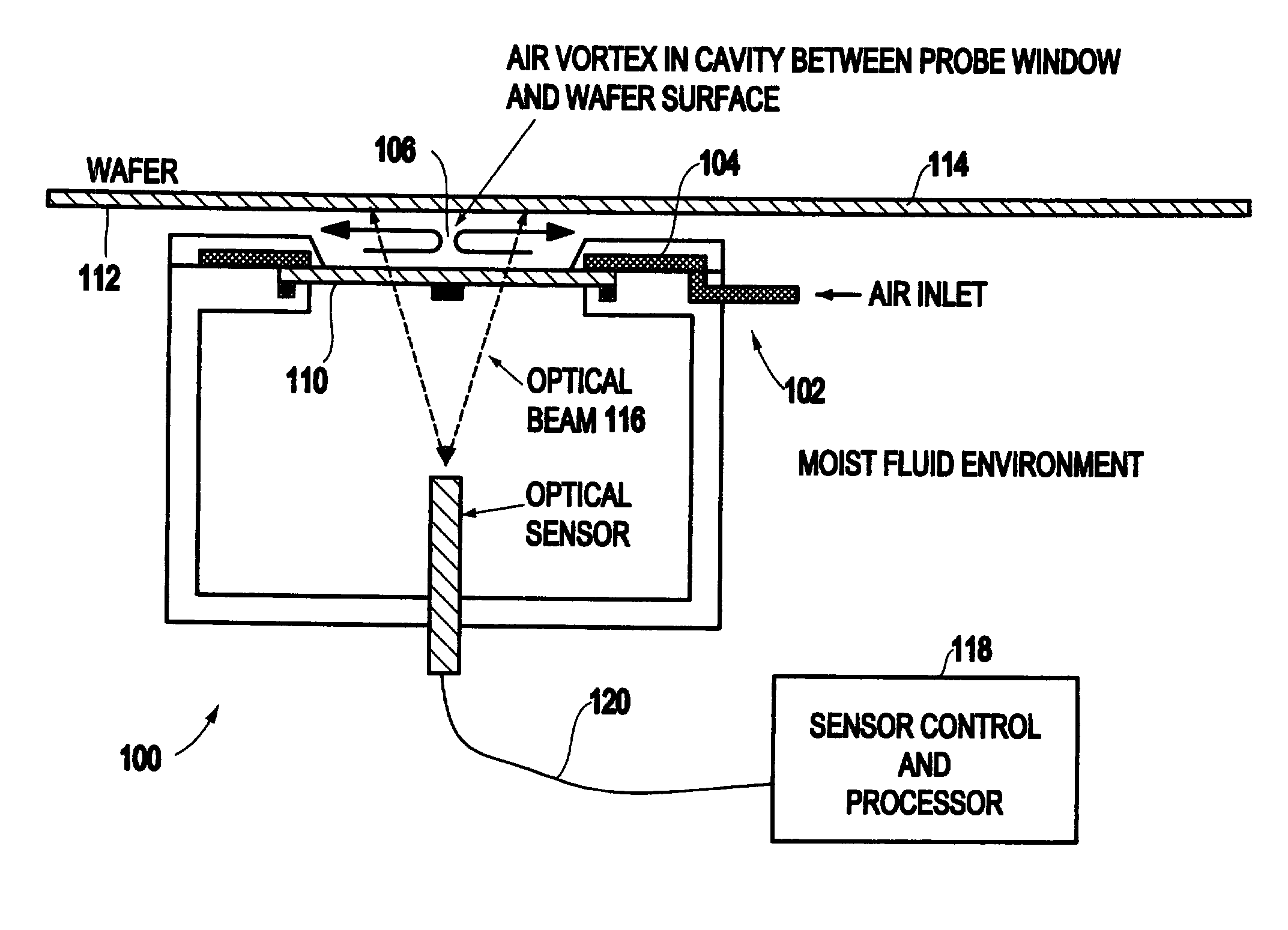
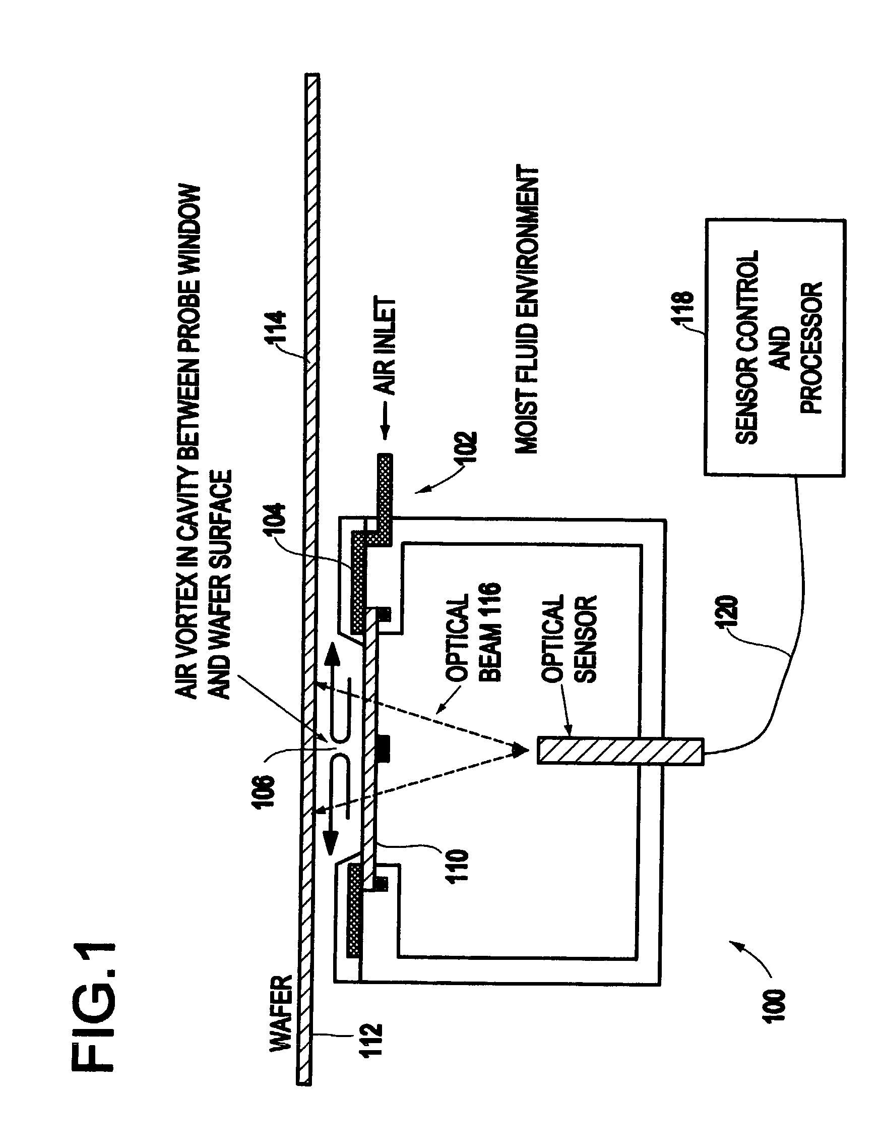
[0023] FIG. 1 illustrates the construction of an exemplary embodiment of a probe 100 in accordance with the present invention. As shown in the Figure, the probe 100 is operating in a moist fluid environment. The moist fluid environment may include any fluid or substance through which the probe 100 penetrates to a surface 112 to be measured. One example of a substance is water.

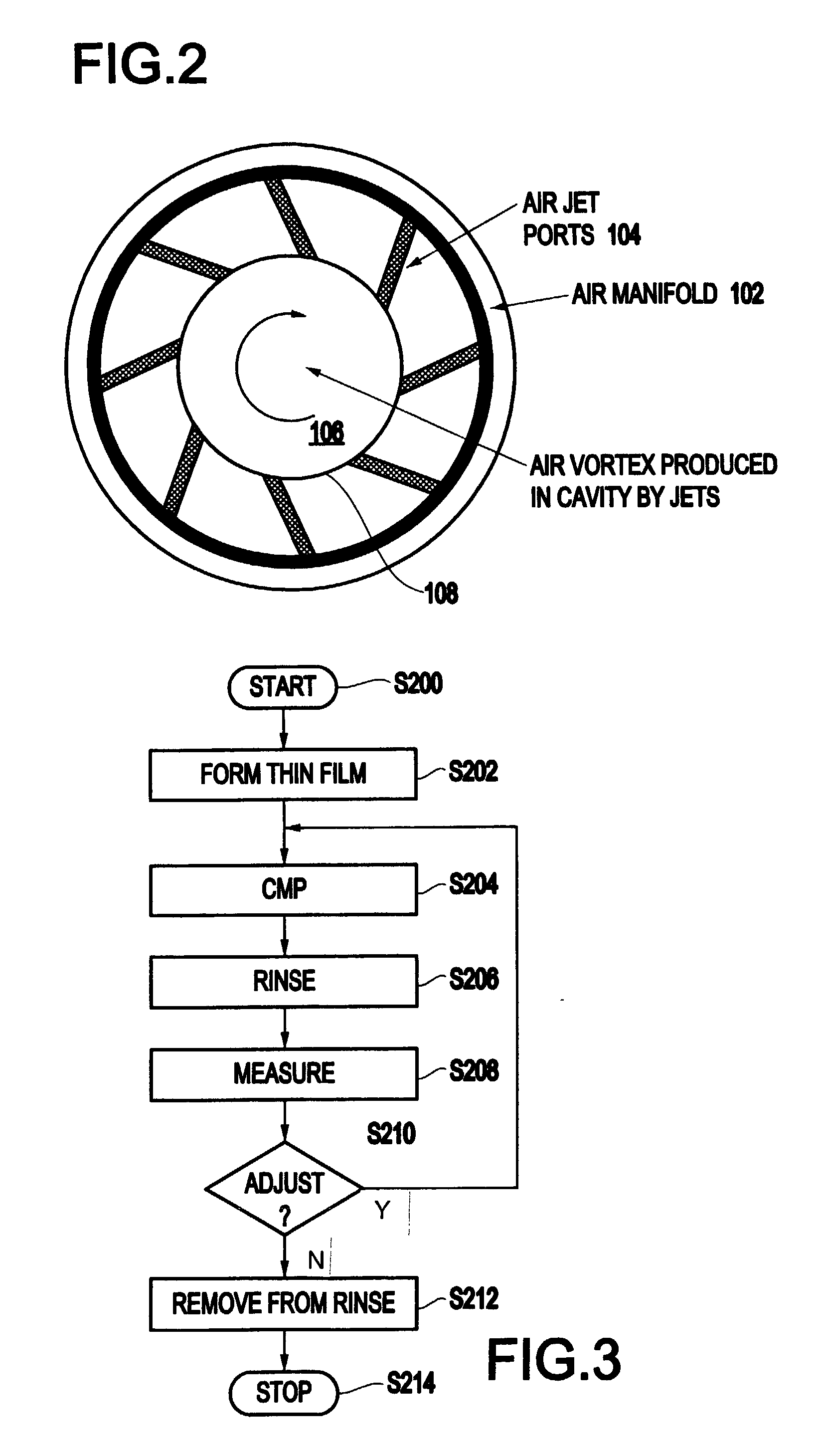
[0024] Air is introduced into a manifold 102 containing multiple jet nozzles 104 which direct the airflow into a vortex 106 in a cavity area 108 between a probe window 110 and a surface 112 of a wafer 114 containing the surface film to be measured.

[0025] The air-vortex 106 created by the air from the nozzles 104 displaces any moisture from the window 110 and the surface 112 of the wafer 114 and blows it to the side. The probe 100 is held in place in a mount (not shown) such that it is in close proximity (e.g., preferably with a gap of about 0.5 mm) to the wafer 114.

[0026] An optical beam 116 is emitted from a f...


PUM

PropertyMeasurementUnit
of timeaaaaaaaaaa
areaaaaaaaaaaa
thicknessaaaaaaaaaa

Abstract

An optical probe (and method) for measuring a surface in an environment containing a first substance, includes a light source for transmitting a light onto an area of the surface to obtain a measurement, a source of the first substance including one of a fluid and a gas for displacing a second substance from an area of the surface receiving the light, and a measuring device for receiving the light being reflected from the surface and for determining a measurement of the surface based upon the reflected light.

Description

[0001] 1. Field of the Invention[0002] The present invention generally relates to optical measurements in a controlled environment. In particular, the present invention relates to an air coupled probe for optical film measurements in a moist aqueous environment.[0003] 2. Description of the Related Art[0004] Optical film thickness measurements are performed routinely in the semiconductor fabrication and machining processes to control film deposition and removal processes. In particular, chemical mechanical polishing (CMP) is used in semiconductor fabrication. In the CMP process, wafers containing thin films are polished in an aqueous environment to planarize the surface. The CMP process is often performed as a multistep process during which the wafers being polished are kept wet. It is desirable to measure the thickness of the material so that the wafers are not over polished and so that surface planarity may be gauged. Presently, the wafers are first removed from the polishing tool,...

Claims


Application Information

Patent Timeline
Patent Type & Authority Applications(United States)
IPC IPC(8): B08B5/02B24B37/013B24B49/12G01N11/06G01N21/00G01N21/15G01N21/55
CPCB08B5/02G01N2021/151B24B49/12B24B37/013
Inventor LEBEL, RICHARD J.MAURER, FREDRIKSMITH, PAUL H. JR.VAN KESSEL, THEODORE G.WICKRAMASINGHE, HEMATHA K.
Owner TAIWAN SEMICON MFG CO LTD
Why Eureka
Try Eureka