Low cost integrated heater substrate for active optical fiber alignment

a heater substrate and active optical fiber technology, applied in optics, instruments, optical light guides, etc., can solve the problems of high cost of laser welding alignment techniques, optical fiber alignment to opto-electronic devices usually cannot be provided, and the epoxy alignment technique is typically less robust than laser welding and soldering

Inactive Publication Date: 2004-06-17
NORTHROP GRUMAN CORP
View PDF11 Cites 5 Cited by
  • Summary
  • Abstract
  • Description
  • Claims
  • Application Information

AI Technical Summary

Problems solved by technology

However, epoxy alignment techniques are typically less robust than laser welding and soldering, and provide higher coefficients of thermal expansion between the epoxy and the substrate that affect the ability to accurately align the fiber to the opto-electronic device.
However, laser welding alignment techniques are typically high cost because of the many expensive components that are required for the process and the long duration of the alignment cycle time.
However, known soldering

Method used


Image

  • Low cost integrated heater substrate for active optical fiber alignment
  • Low cost integrated heater substrate for active optical fiber alignment
  • Low cost integrated heater substrate for active optical fiber alignment

Examples


Embodiment Construction

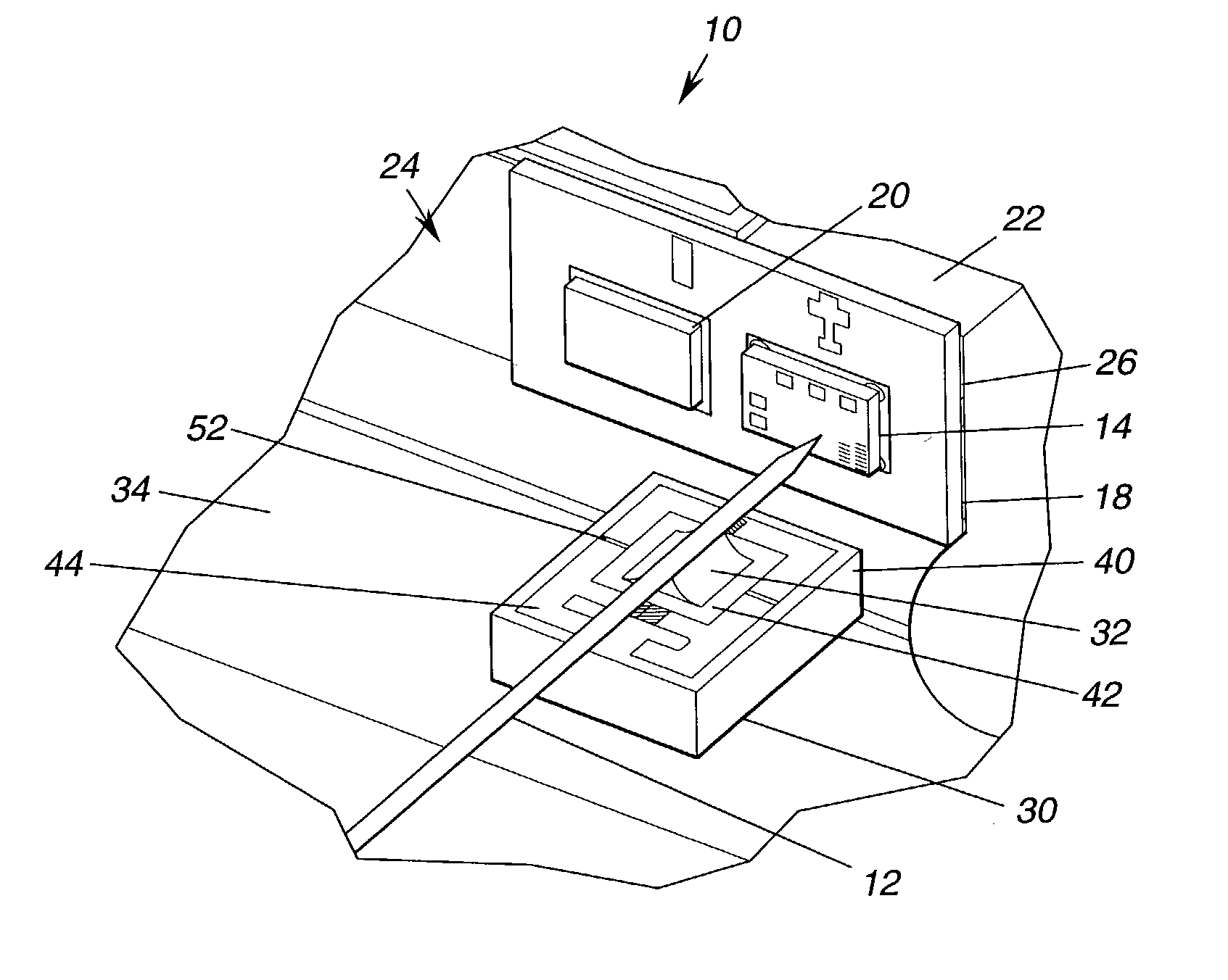
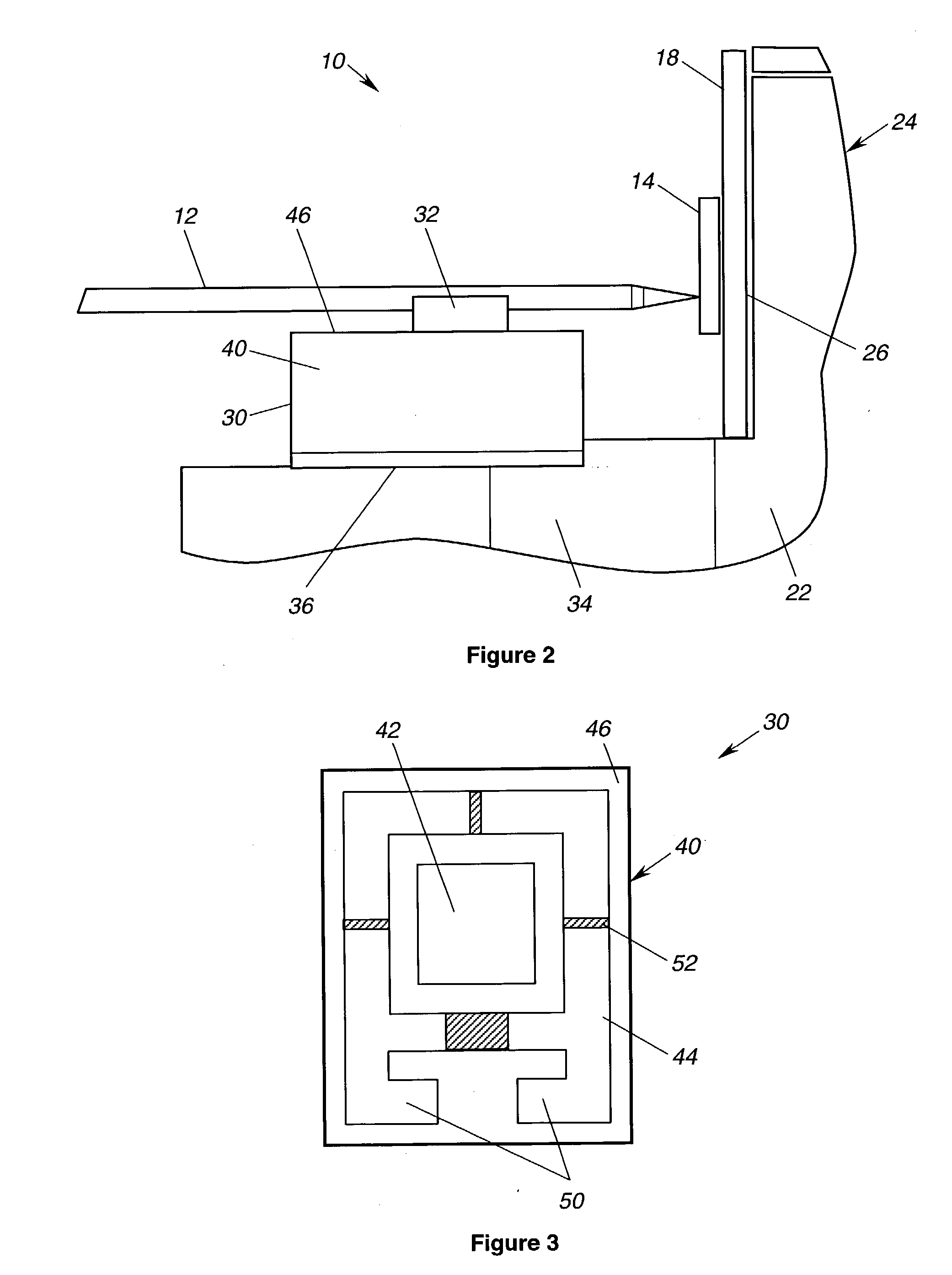
[0018] The following discussion of the embodiments of the invention directed to a soldering technique for aligning an optical fiber to an opto-electronic device is merely exemplary in nature, and is in no way intended to limit the invention or its applications or uses.

[0019] FIG. 1 is a perspective view and FIG. 2 is a side view of an optical packaging assembly 10 that holds an optical fiber 12 in alignment to an opto-electronic device 14. The opto-electronic device 14 can be any suitable optical detector or optical emitter, such as a photodetector or a light emitting diode (LED), employed in an optical communications system. Additionally, the optical fiber 12 can be any suitable optical fiber for such an optical system, such as a single mode or a multi-mode optical fiber. In alternate embodiments, the optical fiber 12 can be mounted within a protective ferrule, or can be other optical waveguides having different shapes, such as rectangular.

[0020] As will be discussed in detail belo...


PUM


Abstract

An optical packaging assembly (10) for securing an optical fiber (12) to a heater substrate (30) in optical alignment with an opto-electronic device (14). The opto-electronic device (14) is secured to a device substrate (18) in the packaging assembly (10). The heater substrate (30) includes a conductive region (44), resistive elements (52) and a solder platform (42). The optical fiber (12) and a solder preform (32) are positioned on the solder platform (42). A voltage potential is applied to the conductive region (44) to heat the resistive elements (52) to cause the solder preform (32) to melt and secure the optical fiber (12) to the heater substrate (30) in alignment with the opto-electronic device (14). The resistive elements (52) are symmetrically disposed around the solder platform (42) to minimize translational and rotational shifts of the optical fiber (12) to primarily one translational axis of motion when the solder preform (32) cools.

Description

[0001] 1. Field of the Invention[0002] This invention relates generally to an opto-electronic assembly for aligning an optical fiber to an opto-electronic device and, more particularly, to an opto-electronic assembly employing a thin-film substrate including an integrated heater, where the heater melts a solder preform to secure an optical fiber in optical alignment with an opto-electronic device.[0003] 2. Discussion of the Related Art[0004] High data rate optical communications systems typically require that an optical fiber or optical waveguide be actively aligned to an opto-electronic device, such as a photoemitter or photodetector, at the applicable locations in the system. Active alignment of an optical fiber to an opto-electronic device uses a sensing system having a feedback loop to indicate that the optical fiber is in precise alignment with the opto-electronic device within minimum tolerances. Passive optical alignment techniques can be employed in low data rate application...

Claims


Application Information

Patent Timeline
IPC IPC(8): G02B6/42
CPCG02B6/4225G02B6/4238G02B6/4226
Inventor MARQUEZ, CHRISTIAN L.LAU, JAMES C.HAMILTON, PAUL J.
Owner NORTHROP GRUMAN CORP
Why Eureka
Try Eureka