Semiconductor device and method for manufacturing same

a technology of semiconductor devices and semiconductors, applied in semiconductor devices, semiconductor/solid-state device details, electrical apparatus, etc., can solve the problems of increasing the problem of electromigration due to mass transfer through particle boundaries, affecting the life of devices with poor electromigration resistance, and affecting the generation of electromigration

Active Publication Date: 2004-07-08
RENESAS ELECTRONICS CORP
View PDF5 Cites 40 Cited by
  • Summary
  • Abstract
  • Description
  • Claims
  • Application Information

AI Technical Summary

Problems solved by technology

On the contrary, the generation of electromigration becomes a problem even in the application of interconnects made of copper, as the reduction of the semiconductor devices is further proceeds.
When an electrical voltage is applied to the copper interconnect having such configuration, mass transfer is occurred through the grain boundaries of the copper particles, resulting in causing the electromigration.
Since the interconnect having smaller line width includes smaller grain sizes of the copper particles, the problem of the electromigration due to the mass transfer through the particle boundaries becomes more serious.
The resistance to the electromigration is closely related to the lifetime of the devices, and devices having poor electromigration resistance tend to have shorter lifetime.
The generation of such void causes an insufficient coupling between the coupling plug and the interconnect, reducing the process yield of the semiconductor device, or destabilizing the operation of the semiconductor device in the long term operation.
However, the technology disclosed in JP-A-H11-204,524 has problems of the increase in the electrical conductivity of the copper interconnect or the like.
In addition, it is difficult to improve the stress migration by this technology, even though this technology is useful in improving the electromigration at certain level.
However, it is still difficult to completely prevent the stress migration even in employing the constitution of forming the silicide layer thereon.
The configuration of being provided with the silicide may not provide sufficient stress migration resistance, as described later.
Excessively larger atomic radius relative to the lattice constant may lead to a difficulty in forming the preferable solid solution layer that preferably meets the object of the present invention, resulting in achieving insufficient improvements in the electromigration resistance and in the stress migration resistance.

Method used


Image

  • Semiconductor device and method for manufacturing same
  • Semiconductor device and method for manufacturing same
  • Semiconductor device and method for manufacturing same

Examples


example 2

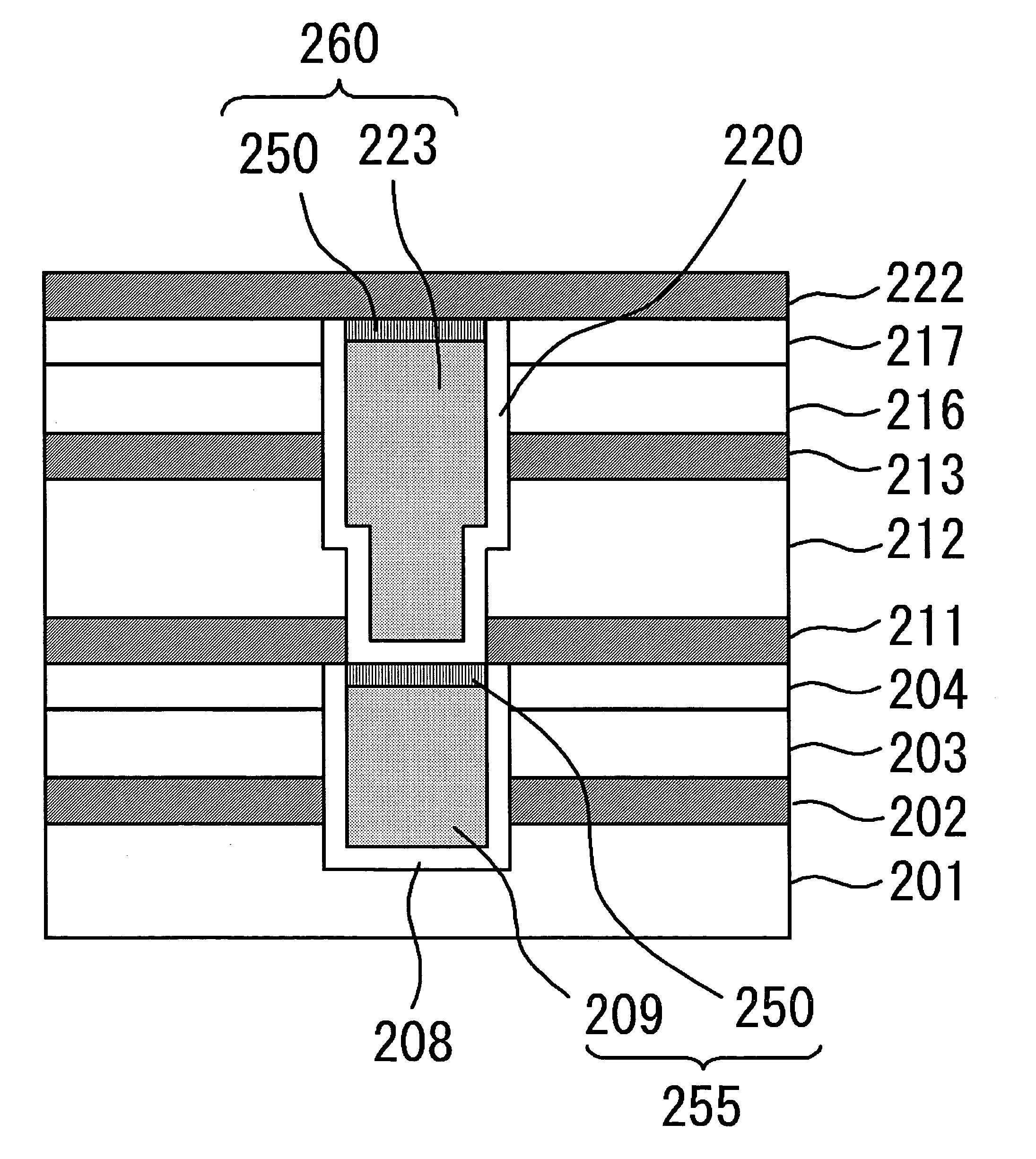
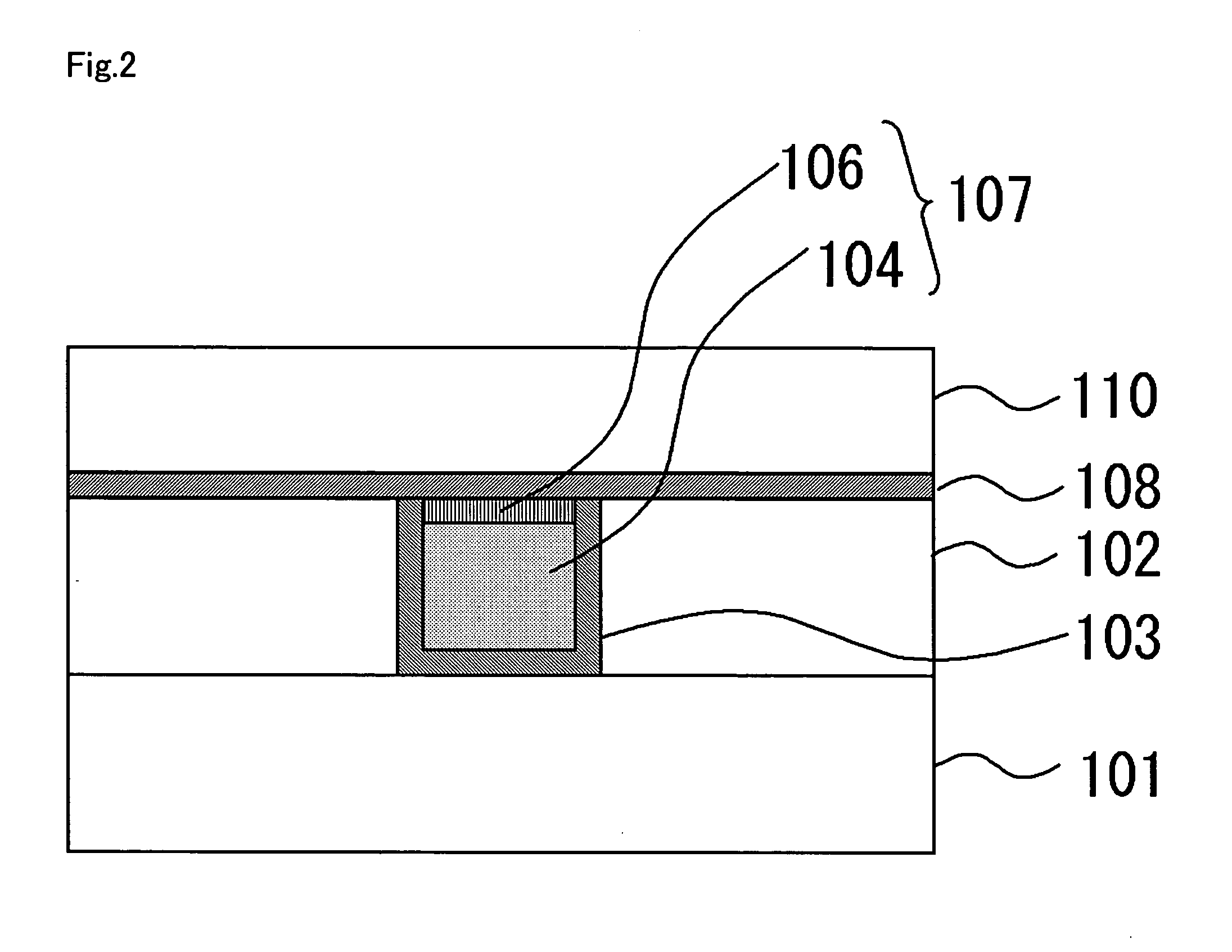
[0124] In this example, dual-layer copper interconnect structures comprising an underlying M1 interconnect and an upper M2 interconnect coupled to the M1 interconnect line through a via as shown in FIG. 19 were manufactured, and process yield tests were performed. The following two samples of the interconnect structures were prepared and evaluated.

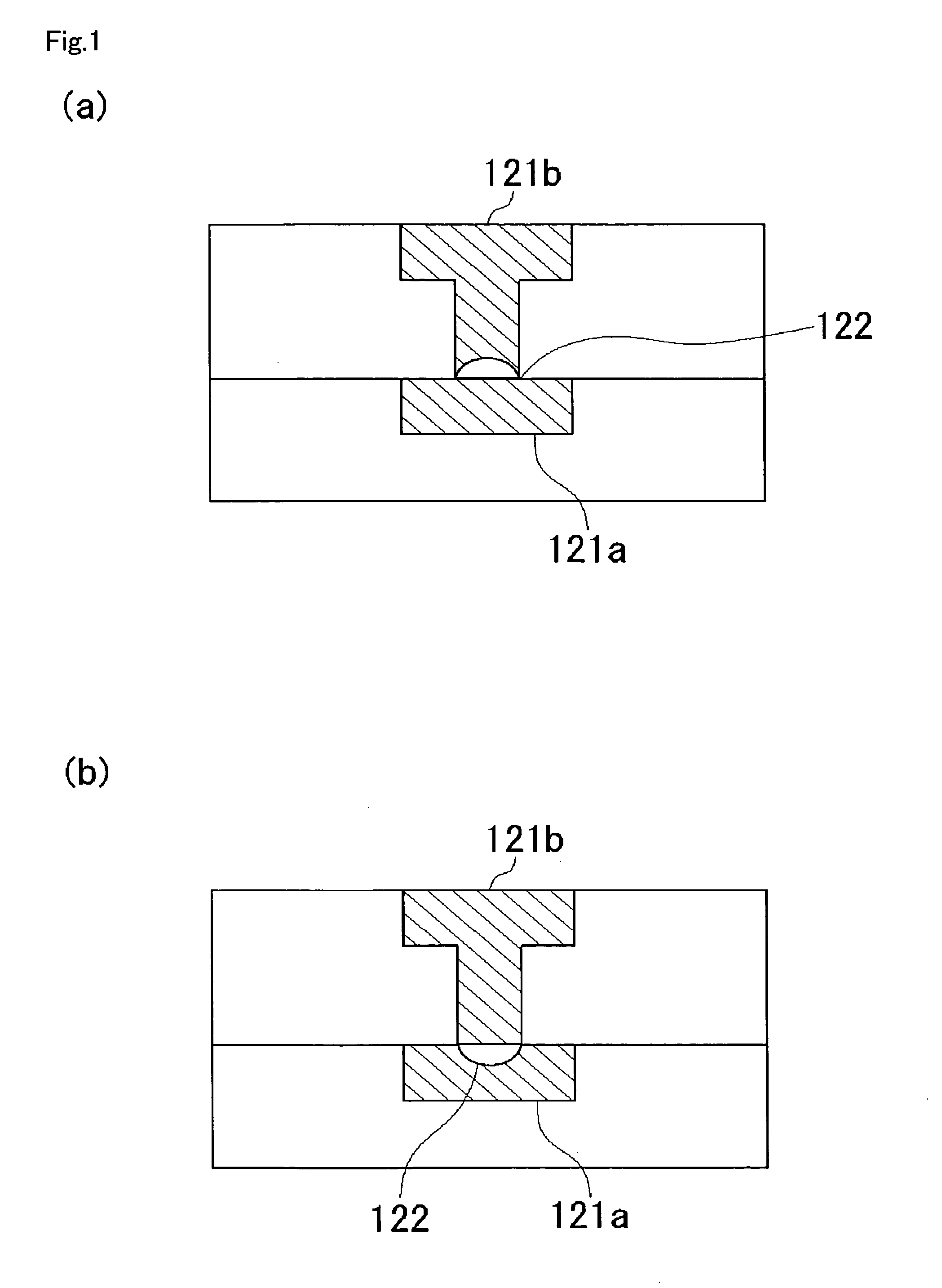
[0125] Sample (i): an interconnect structure prepared by a method similar to the method of the above described second preferred embodiment. Surfaces of the underlying M1 interconnect and the upper M2 interconnect were treated in accordance with a method similar to that used for treating the sample 2 in the Example 1.

[0126] Sample (ii): an interconnect structure prepared by a method generally similar to the method of the above described second preferred embodiment, except that the conditions for the exposure to silane and the conditions for the treatment with oxalic acid and the subsequent rinse processing and so on are modified to form cop...

example 3

[0130] FIG. 21 is a graph showing the results of the evaluation for the process yield of the via chain having the dual-layer interconnect structure. It was found that the sample (i), in which copper is solid-solute within copper, exhibited the better process yield than that of the silicide copper interconnect.

[0131] As described above, the present invention provides the semiconductor device comprising the metal interconnect, which exhibit the considerably improved electromigration resistance and / or stress migration resistance. Therefore, the semiconductor device having improved device lifetime is obtainable by having the configurations of the present invention.


PUM

PropertyMeasurementUnit
atomic radiusaaaaaaaaaa
lattice constantaaaaaaaaaa

Abstract

The present invention provides a semiconductor device comprising a metal interconnect having considerably improved electromigration resistance and / or stress migration resistance. The copper interconnect 107 comprises a silicon-lower concentration region 104 and a silicon solid solution layer 106 disposed thereon. The silicon solid solution layer 106 has a structure, in which silicon atoms are introduced within the crystal lattice structure that constitutes the copper interconnect 107 to be disposed within the lattice as inter-lattice point atoms or substituted atoms. The silicon solid solution layer 106 has the structure, in which the crystal lattice structure of copper (face centered cubic lattice; lattice constant is 3.6 angstrom) remains, while silicon atoms are introduced as inter-lattice point atoms or substituted atoms.

Description

[0001] This application is based on Japanese patent application NO.2002-379278, the content of which is incorporated hereinto by reference.1. FIELD OF THE INVENTION[0002] The present invention relates to a semiconductor device comprising a metal interconnect, and a method for manufacturing same.2. DESCRIPTION OF THE RELATED ART[0003] In recent years, for the purpose of satisfying the increasing requirements for obtaining higher level of the integration of semiconductor devices, copper becomes to be widely employed for material of interconnects or plugs. Copper is a material, which is characterized in having lower resistance and better electromigration resistance than that of aluminum that has been conventionally employed.[0004] On the contrary, the generation of electromigration becomes a problem even in the application of interconnects made of copper, as the reduction of the semiconductor devices is further proceeds. The copper film that constitutes the copper interconnect is gener...

Claims


Application Information

Patent Timeline
Patent Type & Authority Applications(United States)
IPC IPC(8): H01L21/3205H01L21/768H01L23/52H01L23/532
CPCH01L21/76801H01L21/76808H01L21/76849H01L21/76855H01L23/53295H01L21/76867H01L21/76886H01L23/53238H01L23/5329H01L21/76856H01L2924/0002H01L2924/00
Inventor KUNIMUNE, YORINOBUHASEGAWA, MIEKOITOU, TAKAMASATAKEDA, TAKESHIAOKI, HIDEMITSU
Owner RENESAS ELECTRONICS CORP
Why Eureka
Try Eureka