Diffuser plate and method of making same

a diffuser plate and plate technology, applied in the field of extreme short wavelength photolithography systems, can solve the problems of degrading circuit patterns created on silicon wafers, unable to work at such short wavelengths, and various problems,

Active Publication Date: 2004-07-15
ASML HLDG NV
View PDF10 Cites 5 Cited by
  • Summary
  • Abstract
  • Description
  • Claims
  • Application Information

AI Technical Summary

Problems solved by technology

However, constantly shrinking wavelengths have yielded a number of challenges to chip manufacturers.
As a result of this phenomenon, some light may fail to reach the silicon wafer, resulting in a degraded circuit pattern being created on the silicon wafer.
The pro

Method used


Image

  • Diffuser plate and method of making same
  • Diffuser plate and method of making same
  • Diffuser plate and method of making same

Examples


Embodiment Construction

[0022] Reference will now be made in detail to the embodiments of the present invention, examples of which are illustrated in the accompanying drawings.

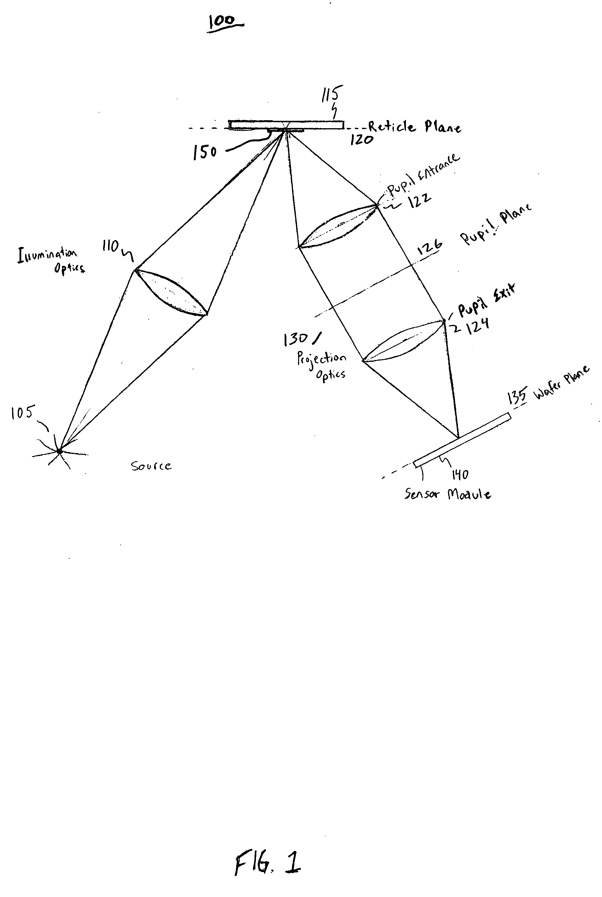
[0023] FIG. 1 illustrates a portion of a representative photolithographic system 100. System 100 is shown in a system test configuration. A source 105 provides electromagnetic radiation to the illumination optics 110. In the exemplary EUV embodiment, the illumination optics are reflective because of the very short EUV wavelengths. The illumination optics 110 focus the electromagnetic radiation on a reticle stage (not shown) which is located at the reticle plane 120. A reticle stage (not shown) ordinarily holds the reticle during lithography. Instead of a reticle mounted at the reticle plane 120, a source module 115 is mounted. This is preferred for initial system setup. The test configuration is also preferred for system diagnostics if the system capabilities are reduced during lithography as a result of thermal distortions or elemen...


PUM


Abstract

An electromagnetic radiation diffuser, operative at extreme ultraviolet (EUV) wavelengths, is fabricated on a substrate. The diffuser comprises a randomized structure having a peak and valley profile over which a highly reflective coating is evaporated. The reflective coating substantially takes the form of the peak and valley profile beneath it. An absorptive grating is then fabricated over the reflective coating. The grating spaces will diffusely reflect electromagnetic radiation because of the profile of the randomized structure beneath. The absorptive grating will absorb the electromagnetic radiation. The grating thus becomes a specialized Ronchi ruling that may be used for wavefront evaluation and other optical diagnostics in extremely short wavelength reflective lithography systems, such as EUV lithography systems.

Description

[0001] This application claims the benefit of U.S. Provisional Appl. No. 60 / 440,053, filed Jan. 15, 2003 (incorporated in its entirety herein by reference).[0002] 1. Field of the Invention[0003] The present invention is generally related to extremely short wavelength photolithography systems and, more particularly, to diffusely reflecting electromagnetic radiation in extreme ultraviolet (EUV) lithography systems.[0004] 2. Related Art[0005] Lithography is a process used to create features on the surface of substrates. Lithography is a well known process in the art of manufacturing computer chips. A frequently used substrate for computer chips is a semiconductor material such as silicon or gallium arsenide. During lithography, a semiconductor wafer situated on a stage within a lithography tool is exposed to an image projected onto the surface of the wafer by an exposure system. The exposure system typically includes a reticle (also called a mask) for projecting an image of circuit fea...

Claims


Application Information

Patent Timeline
IPC IPC(8): G02B5/02G02B5/08G02B5/18G21K1/06G03F7/20H01L21/027
CPCG03F7/706G02B5/1838G03F7/7085
Inventor AUGUSTYN, WALTER H.GONTIN, RICHARD A.
Owner ASML HLDG NV
Why Eureka
Try Eureka