
Positron emission tomography device

a tomography and positron emission technology, applied in the direction of radiation intensity measurement, instruments, x/gamma/cosmic radiation measurement, etc., can solve the problems of complex computational processing, inability to determine the disappearance position of the tracer within this width, and slowdamping time of about 300 ns

Inactive Publication Date: 2004-09-09
JAPAN SCI & TECH CORP
View PDF5 Cites 13 Cited by
  • Summary
  • Abstract
  • Description
  • Claims
  • Application Information

AI Technical Summary

Benefits of technology

[0012] It was discovered that by using this scintillator as a .gamma.-ray detector of a positron emission tomography device, the problems inherent in the positron emission tomography device of the related art could be solved.

Problems solved by technology

Of these, the .gamma.-ray detection efficiency of BGO is high and it is therefore often used, but it has the fault that the damping time is as slow as about 300 ns.
If the response time of the scintillator used as PET detector is slow, and the signal from the detector has a fairly large width over time, the disappearance position of the tracer cannot be determined within this width.
With the newest PET devices, the spatial resolving power is increasing, but complex computational processing is required.
As the response speed of the scintillator used in the prior art positron emission tomography device was extremely limited, there was also a limit to the resolution of the positron emission tomography device.
If R.sup.1-R.sup.4 contain unsaturated bonds such as double bonds or triple bonds, high energy radiation is absorbed causing radical reactions, which is undesirable.
If the photomultiplier is made small on the other hand, there is a problem that performance falls.

Method used


Image

  • Positron emission tomography device
  • Positron emission tomography device
  • Positron emission tomography device

Examples


example 2

[0060] A stratified perovskite compound (C.sub.6H.sub.13NH.sub.3).sub.2PbI-.sub.4 was synthesized by reacting lead iodide, PbI.sub.2, as metal halide, with C.sub.6H.sub.13NH.sub.3I as organoamine halide acid salt in a molar ratio of 1:2, in N,N-dimethylformamide (reaction temperature: room temperature (20.degree. C.), reaction time: 1 hour or more).

[0061] 1 g of this stratified perovskite compound was dissolved in 3 ml of acetone, and spin-coated onto a silicone (Si) substrate of 2 cm side using a Shimadzu P / N 202-32016 (rotation speed: 5000 rpm, time: 30 seconds or more), so as to manufacture a scintillator (thickness of stratified perovskite compound, 0.1 micrometers). Herein, a silicon substrate is used to avoid luminescence from the substrate.

[0062] The radiation detector used in this measurement example comprises a cylindrical stainless steel pillar having a diameter of approx. 50 cm, and provided with a window on which the radiation is incident, light-receiving port, sample ho...


PUM

PropertyMeasurementUnit
γ-aaaaaaaaaa
decay time constantaaaaaaaaaa
temperatureaaaaaaaaaa

Abstract

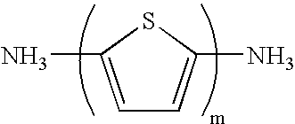
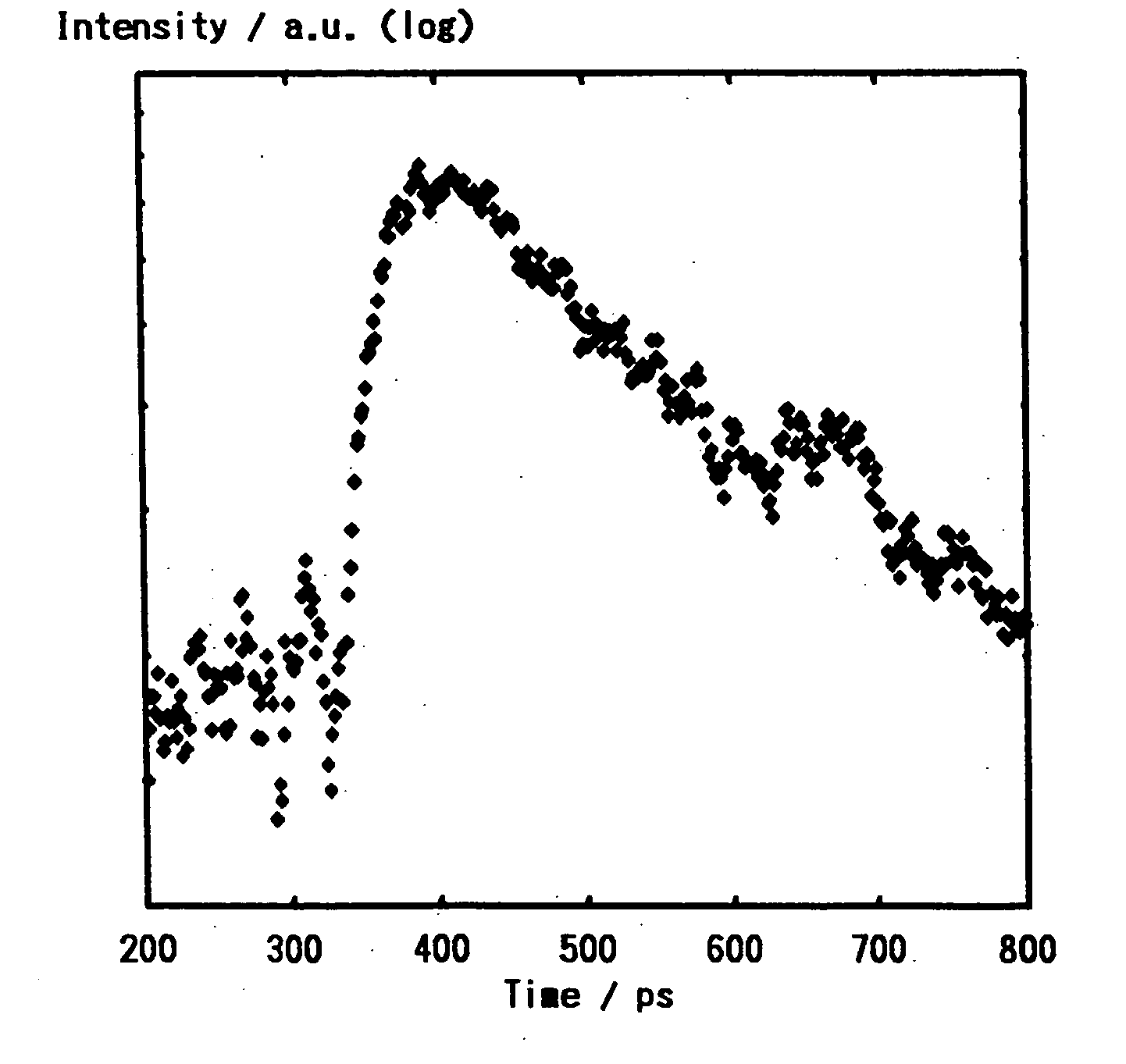
As the response speed of the scintillator used in the prior art positron emission tomography device was extremely limited, there was a limit to the resolution of the positron emission tomography device. To resolve this problem, it was considered that the scintillator should have a response speed of approx. 10<-10 >seconds (0.1 ns). If such a scintillator can be manufactured, a time-of-flight PET can be realized. The inventor already discovered that if a specific perovskite organic / inorganic hybrid compound is used as a radiation scintillator, it emits visible light with a very fast (subnanosecond order) response, and that this scintillator can be used as the gamma-ray detector of the positron emission tomography device. The PET device of this invention comprises as a scintillator a perovskite organic / inorganic hybrid compound selected from the group represented by the general formulae: (R<1>-NR<11>3)2MX4 or (R<2>-NR<12>)2MX4, (NR<13>3-R<3>-NR<13>3)MX4 or (NR<14>2=R<4>=NR<14>2)MX4, or AMX3.

Description

[0001] This invention relates to a positron emission tomography device, and more specifically, to a positron emission tomography device using a .gamma.-ray detector comprising a very fast (of the order of nanoseconds or less) scintillator.PRIOR ART[0002] Positron emission tomography (henceforth "PET"), is a tomographic method used for nuclear medical diagnosis wherein a subject is given a radioactive drug (tracer) labeled by a positron radiator, the radiation emitted outside the body is measured, and the concentration distribution of the drug is measured as a tomogram. ("Medical Imaging Handbook" (1994); RADIOISOTOPES, 42, 189-198; (1993) RADIOISOTOPES, 42, 237-254); (1993) RADIOISOTOPES, 42, 301-314; (1993) RADIOISOTOPES, 42, 365-376 (1993).[0003] The positrons emitted from the tracer (atomic nucleus) travel several millimeters inside the body, lose kinetic energy, collide with nearby electrons and disappear. At this time, .gamma.-rays (511 keV) having an energy equivalent to the e...

Claims


Application Information

Patent Timeline
Patent Type & Authority Applications(United States)
IPC IPC(8): C09K11/06G01T1/20G01T1/161G01T1/202
CPCC09K11/06C09K2211/188C09K11/664
Inventor SHIBUYA, KENGOKOSHIMIZU, MASANORIASAI, KEISUKE
Owner JAPAN SCI & TECH CORP
Learn More