Semiconductor Detector Block and Positron Emission Tomography Device Using the Same

a technology of positron emission tomography and semiconductor detectors, which is applied in the direction of x/gamma/cosmic radiation measurement, radiofrequency measurement devices, instruments, etc., can solve the problems of difficult use of ge and si for the semiconductor detectors of the positron emission tomography apparatus, and insufficient absorption effect of gamma rays having energies of 511 kev, etc., to achieve the effect of simple detector structur

Inactive Publication Date: 2011-02-24
SUMITOMO HEAVY IND LTD
View PDF5 Cites 9 Cited by
  • Summary
  • Abstract
  • Description
  • Claims
  • Application Information

AI Technical Summary

Benefits of technology

[0008]Accordingly, it is a general object of the present invention to provide a novel and useful semiconductor detector block having a simple detector structure and performing a measurement with a spatial resolution (the accuracy of the position resolution) of 1 mm or less, and a positron emission tomography apparatus having the semiconductor detector block.

Problems solved by technology

Although there are proposed examples of semiconductor detectors using Ge, Si, or the like, these examples need cooling with liquid nitrogen and an absorption effect for gamma rays having energies of 511 keV is insufficient since the atomic numbers of Ge and Si are smaller than the atomic number of the CdTe.
Therefore, it is difficult to use Ge and Si for the semiconductor detectors of the positron emission tomography apparatus.

Method used


Image

  • Semiconductor Detector Block and Positron Emission Tomography Device Using the Same
  • Semiconductor Detector Block and Positron Emission Tomography Device Using the Same
  • Semiconductor Detector Block and Positron Emission Tomography Device Using the Same

Examples


Embodiment Construction

[0022]A description is given below, with reference to the FIG. 1 through FIG. 4 of embodiments of the present invention.

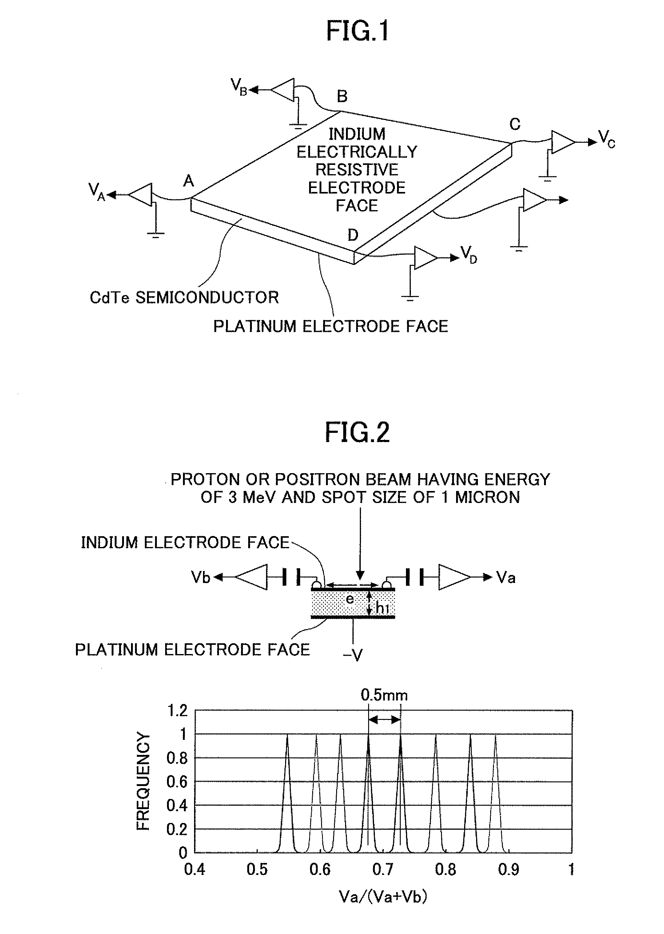
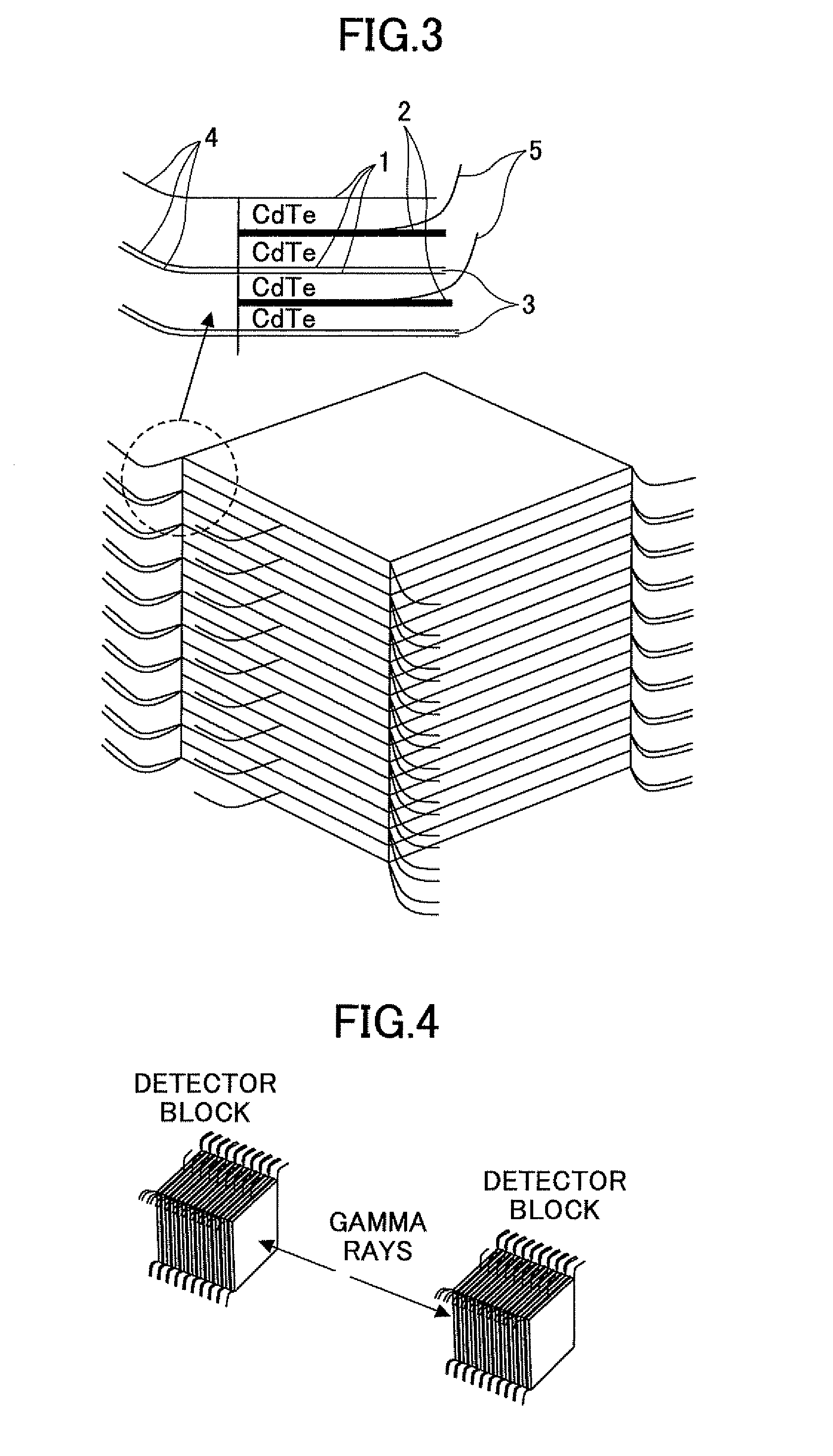
[0023]Reference symbols typically designate as follows:[0024]1: Indium electrically resistive electrode face;[0025]2: Platinum electrically conductive electrode face;[0026]3: Insulating thin film;[0027]4: Terminal of indium electrically resistive electrode face; and[0028]5: Terminal of platinum electrically conductive electrode face.

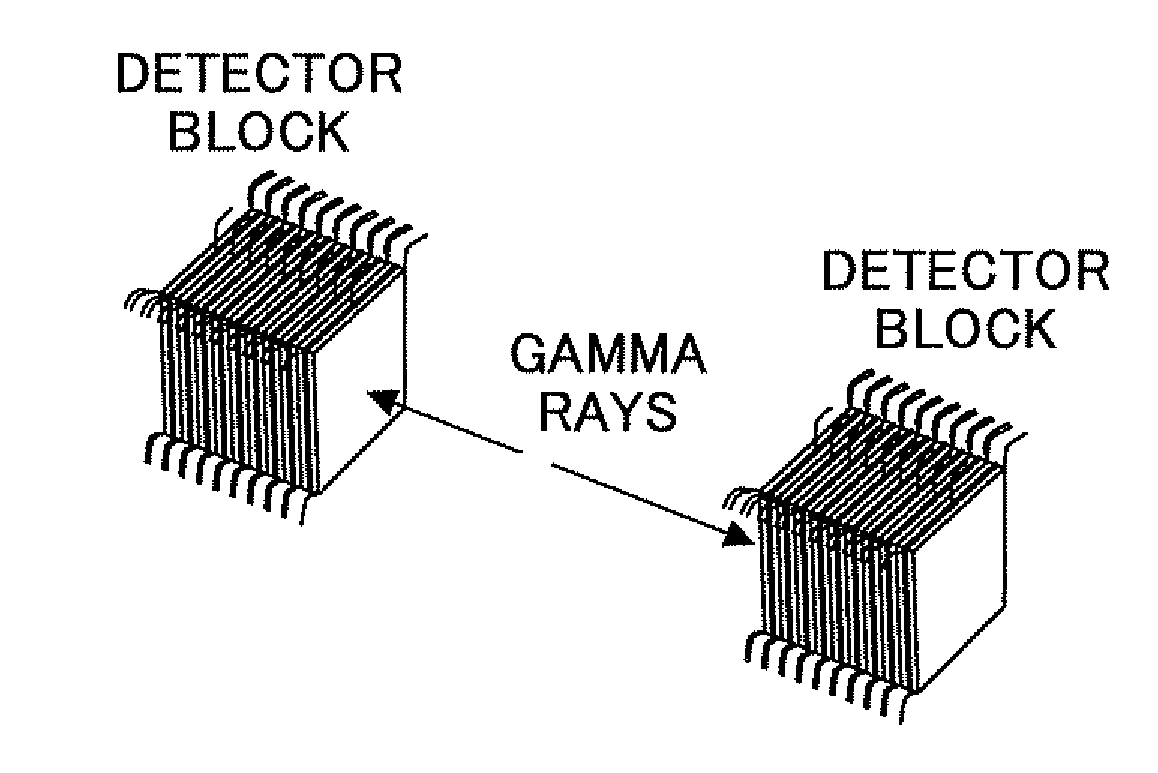
[0029]A semiconductor detector block which can measure a three-dimensional position of gamma rays will be described in detail with reference to the figures. FIG. 1 illustrates a semiconductor detector which can detect a two-dimensional detection position of gamma rays on a semiconductor plate of the semiconductor detector. Referring to FIG. 1, a material of the thin semiconductor crystal plate is a CdTe crystal or a BrTl crystal. One face of the thin semiconductor crystal plate has an electrically resistive electrode, and the other face...


PUM


Abstract

A disclosed semiconductor detector block includes a plurality of semiconductor plates each configured to have a front surface on which an electrically resistive electrode is formed and a back surface on which an electrically conductive electrode is formed and to detect a two-dimensional detection position of gamma rays on the semiconductor plates using a ratio of electric signals from four corners of the electrically resistive electrode, wherein the plurality of semiconductor plates are piled up and a three-dimensional detection position of the gamma rays is detectable using a ratio of the electric signals from the four corners of the electrically resistive electrodes.

Description

CROSS-REFERENCE TO RELATED APPLICATIONS[0001]This application is a U.S. continuation application filed under 35 USC 111a and 365c of PCT application JP2008 / 057968, filed Apr. 24, 2008. The foregoing application is hereby incorporated herein by reference.BACKGROUND OF THE INVENTION[0002]1. Field of the Invention[0003]The present invention generally relates to a semiconductor detector block used for a positron emission tomography device which may be provided for making a diagnosis of cancers or organs like a brain while administering an agent containing a positron-emitting radionuclide, to a positron emission tomography apparatus for development of agents with animal experiments or the like, and to a positron emission tomography apparatus using the semiconductor detector block.[0004]2. Description of the Related Art[0005]A positron emission tomography apparatus detects two gamma rays, each having energy of 511 keV with an angle of 180 degrees between the directions of the two gamma ra...

Claims


Application Information

Patent Timeline
Patent Type & Authority Applications(United States)
IPC IPC(8): G01T1/24G01T1/29
CPCG01T1/249H01L31/02024G01T1/247G01T1/242H01L31/0296
Inventor ISHII, KEIZOKIKUCHI, YOUHEIMATSUYAMA, SHIGEOYAMAZAKI, HIROMICHI
Owner SUMITOMO HEAVY IND LTD
Why Eureka
Try Eureka