Optical recording disk

a recording disk and optical technology, applied in mechanical recording, instrumentation, disposition/mounting of heads, etc., can solve the problems of reading errors, inability to control tracking in a desired manner, and high jitter of a signal obtained by reading data

Inactive Publication Date: 2004-10-14
TDK CORPARATION
View PDF41 Cites 40 Cited by
  • Summary
  • Abstract
  • Description
  • Claims
  • Application Information

AI Technical Summary

Problems solved by technology

However, in the case where the track pitch is made small in this manner, unless the grooves and lands are formed so as to have desired shapes, jitter of a signal obtained by reading data becomes higher, whereby reading errors are liable to occur and tracking cannot be controlled in a desired manner.
In particular, when data recorded in the recording layer farthest from the light transmission layer are reproduced, if the region of the recording layer other than the recording layer farthest from the light transmission layer through which the laser beam passes contains a boundary between a region where a record mark is formed and a blank region, since the distribution of the reflection coefficient is not uniform at the spot of the laser beam, data recorded in the recording layer farthest from the light transmission layer cannot be reproduced in a desired manner.

Method used


Image

  • Optical recording disk
  • Optical recording disk
  • Optical recording disk

Examples


working example 1

[0273] Each of stampers #1 to #19 in which grooves having different depths were formed were fabricated in the following manner.

[0274] First, a coupling agent layer was formed on a glass plate whose surface was polished and a photo-resist layer having a thickness of 12 nm was formed on the coupling agent layer by applying photo-resist onto the coupling agent layer using a spin coating method and baking the photo-resist at 85.degree. C. for twenty minutes, thereby removing residual solvent.

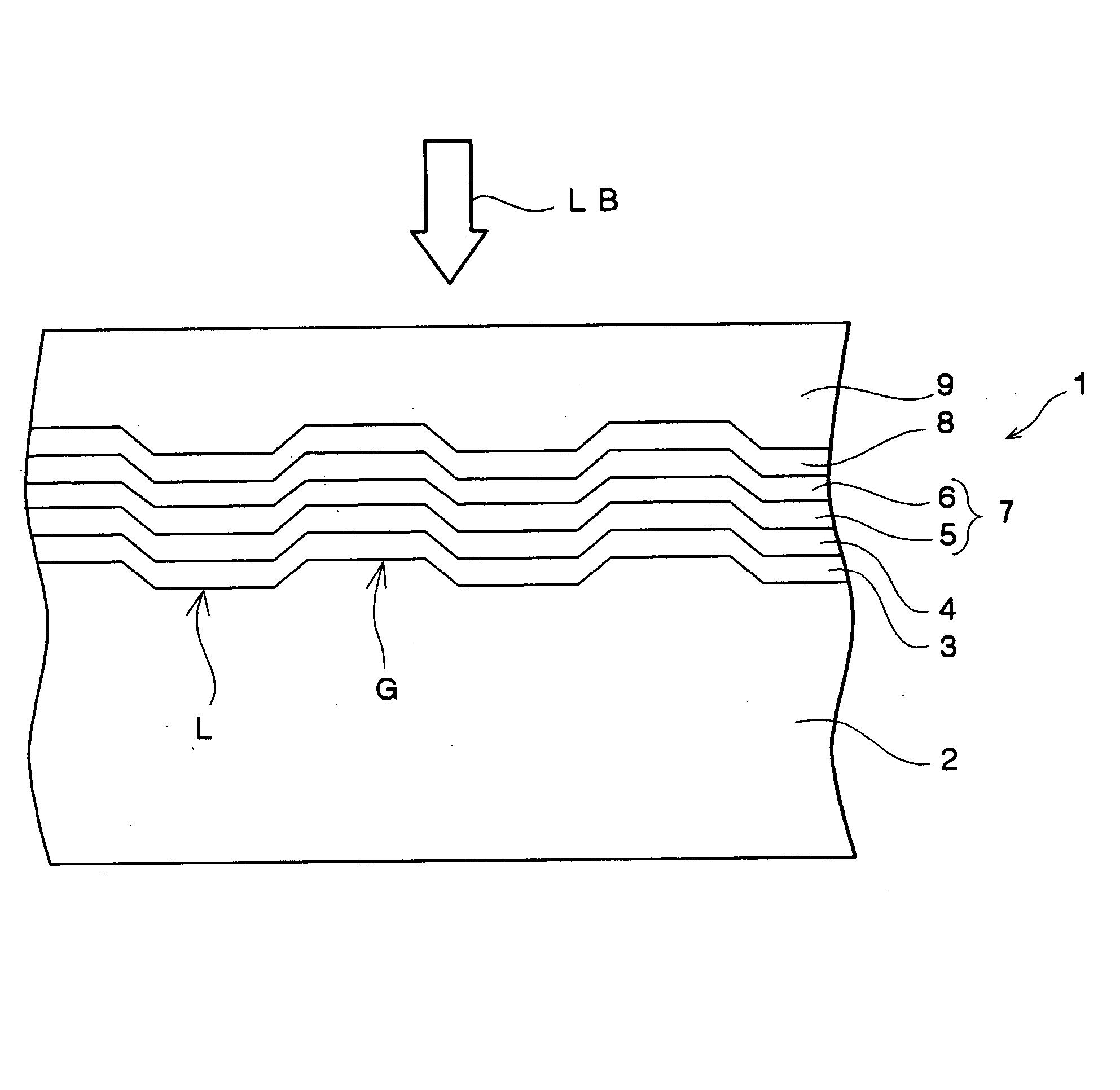
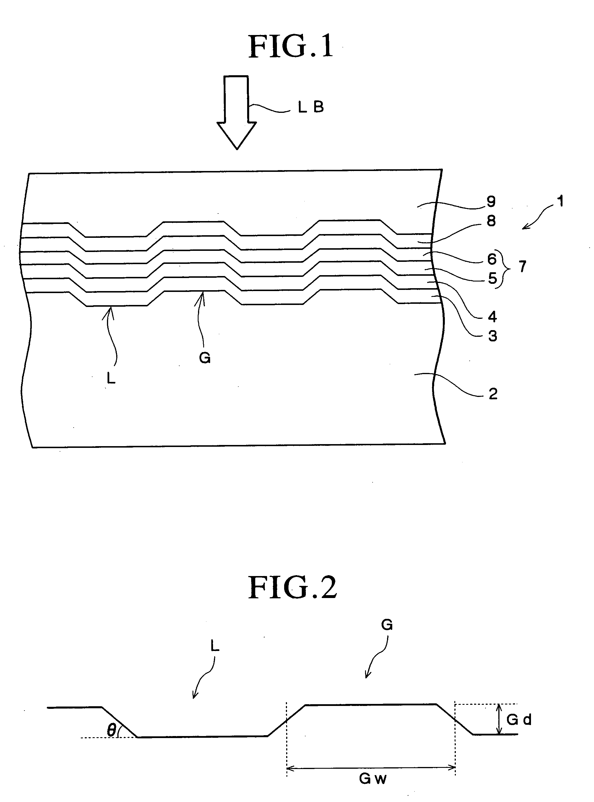
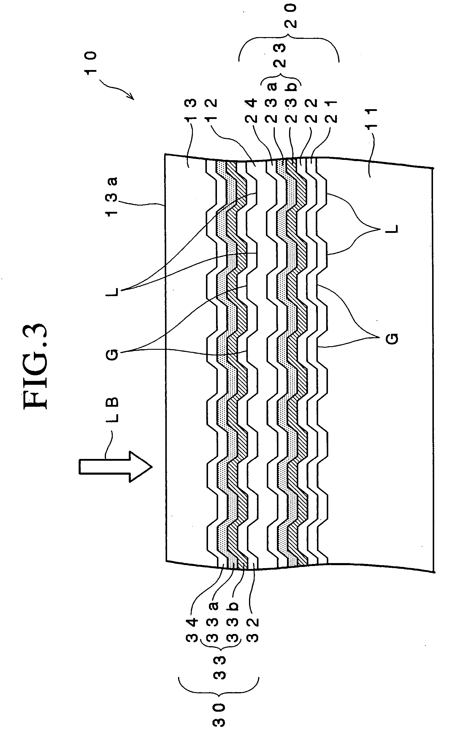
[0275] The photo-resist layer was then exposed to a far ultraviolet laser beam LB having a wavelength of 266 nm with a track pitch of 320 nm using a cutting machine manufactured and sold by Sony Corporation.

[0276] Then, the photo-resist layer was developed to fabricate a photo-resist coated glass board.

[0277] Further, a thin layer of nickel was formed on the photo-resist layer of the photo-resist coated glass board using an electroless plating process.

[0278] A nickel electroformed film was then form...

working example 2

[0296] A stamper #20 formed with grooves having different half widths between zones was fabricated in the following manner.

[0297] First, a coupling agent layer was formed on a glass plate whose surface was polished and a photo-resist layer having a thickness of 22 nm was formed on the coupling agent layer by applying photo-resist onto the coupling agent layer using a spin coating method and baking the photo-resist at 85.degree. C. for twenty minutes, thereby removing residual solvent.

[0298] The photo-resist layer was then exposed to a far ultraviolet laser beam having a wavelength of 266 nm with a track pitch of 320 nm using a cutting machine manufactured and sold by Sony Corporation. The photo-resist layer was exposed to a far ultraviolet laser beam whose power was set different in each zone.

[0299] Then, the photo-resist layer was developed to fabricate a photo-resist coated glass board formed with grooves having different half widths between zones.

[0300] A stamper #20 was fabricat...

working example 3

[0309] A stamper #21 formed with grooves so that the amplitudes Wob of wobbling thereof with respect to an imaginary center line thereof were different between zones was fabricated in the following manner.

[0310] First, a coupling agent layer was formed on a glass plate whose surface was polished and a photo-resist layer having a thickness of 20 nm was formed on the coupling agent layer by applying photo-resist onto the coupling agent layer using a spin coating method and baking the photo-resist at 85.degree. C. for twenty minutes, thereby removing residual solvent.

[0311] The photo-resist layer was then exposed to a far ultraviolet laser beam having a wavelength of 266 nm with a track pitch of 320 nm using a cutting machine manufactured and sold by Sony Corporation so that the half width of each groove was made 170 nm after the development.

[0312] At this time, the amplitude of wobbling of the grooves was varied by changing the voltage input to a wobble setting circuit of the cutting ...


PUM

PropertyMeasurementUnit
half width Gwaaaaaaaaaa

Abstract

An optical recording disk includes a support substrate, grooves and lands alternately formed on one major surface of the support substrate, an optical functioning layer formed on the one major surface of the support substrate on which the grooves and the lands are formed and including a recording layer and a light transmission layer formed on the optical functioning layer, the grooves and the lands being formed so that the depth Gd of each of the grooves is equal to or larger than 15 nm and equal to or smaller than 25 nm and the half width Gw is equal to or larger than 150 nm and is equal to or smaller than 230 nm, and the recording layer including a first recording film containing Si as a primary component and a second recording film containing Cu as a primary component. According to the thus constituted optical recording disk, it is possible to suppress jitter of a signal obtained by reading data within a predetermined range, thereby suppressing reading errors, and it is possible to maintain the level of a push-pull signal equal to or higher than a predetermined value, thereby enabling tracking control in a desired manner.

Description

[0001] The present invention relates to an optical recording disk and, in particular, to an optical recording disk which can suppress jitter of a signal obtained by reading data within a predetermined range, thereby suppressing reading errors, and maintain the level of a push-pull signal equal to or higher than a predetermined value, thereby enabling tracking control in a desired manner.DESCRIPTION OF THE PRIOR ART[0002] Optical recording disks such as the CD, DVD and the like have been widely used as recording media for recording a large amount of digital data.[0003] These optical recording disks can be roughly classified into so-called ROM type optical recording disks such as the CD-ROM and the DVD-ROM that do not enable writing and rewriting of data, so-called write-once type optical recording disks such as the CD-R and DVD-R that enable writing but not rewriting of data, and data rewritable type optical recording disks such as the CD-RW and DVD-RW that enable rewriting of data.[...

Claims


Application Information

Patent Timeline
Patent Type & Authority Applications(United States)
IPC IPC(8): G11B7/007G11B7/09G11B7/243G11B7/258G11B7/26
CPCG11B7/00718G11B7/24038G11B7/24076G11B7/24079G11B7/24082G11B7/243G11B7/258G11B7/266
Inventor OYAKE, HISAJIKAWAGUCHI, YUUICHITAKAHATA, HIROAKIMISHIMA, KOUJIINOUE, HIROYASUKOMAKI, TSUYOSHIAOSHIMA, MASAKIKAKIUCHI, HIRONORI
Owner TDK CORPARATION
Why Eureka
Try Eureka