Ion implantation in channel region of CMOS device for enhanced carrier mobility

Inactive Publication Date: 2004-10-21
LSI CORPORATION
View PDF25 Cites 12 Cited by
  • Summary
  • Abstract
  • Description
  • Claims
  • Application Information

AI Technical Summary

Benefits of technology

0008] The present invention involves ion implantation into a silicon (Si) substrate to enhance carrier mobility in the channel region of CMOS devices in an integrated circuit (IC). Heretofore, such ion implantation has been known to be used to enhance source and drain performance in CMOS devices as a pre-amorphization step, but has not been used to affect channel performance. By enhancing carrier mobility in the channel according to the

Problems solved by technology

Heretofore, such ion implantation has been known to be used to enhance source and drain performanc

Method used


Image

  • Ion implantation in channel region of CMOS device for enhanced carrier mobility
  • Ion implantation in channel region of CMOS device for enhanced carrier mobility
  • Ion implantation in channel region of CMOS device for enhanced carrier mobility

Examples


Embodiment Construction

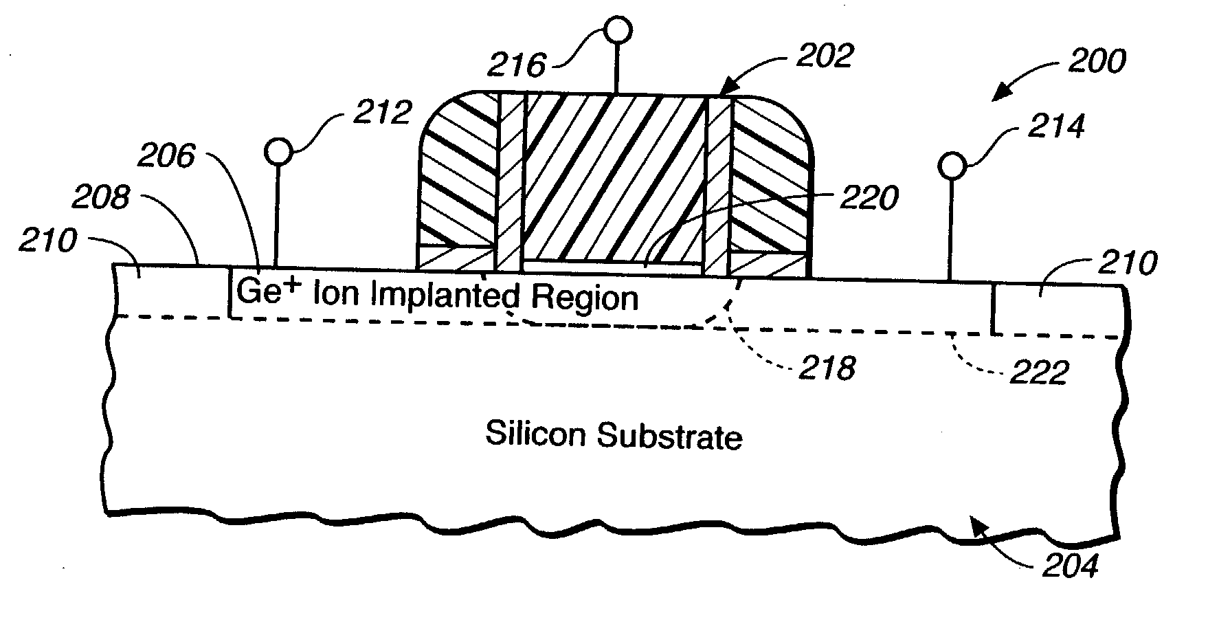
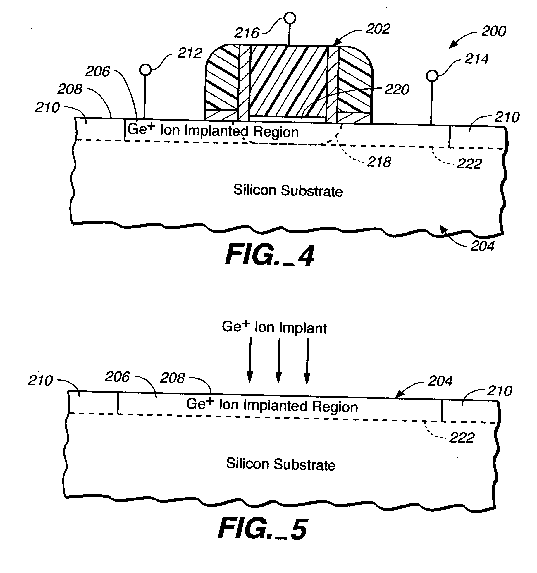
[0018] A portion of an integrated circuit (IC) 200 which incorporates the present invention and which is formed by the methodology of the present invention is shown in FIG. 4. The IC 200 includes a CMOS device 202 (such as a conventional CMOS transistor) formed on a silicon (Si) substrate 204 preferably, though not necessarily, with sub-0.1 micron technology. The Si substrate 204 generally includes an ion-implanted region 206 that extends below the surface 208 of the Si substrate 204. The Si substrate 204 may also include a conventional non-implanted region 210. The CMOS device 202 generally includes a source 212 and a drain 214 which are formed on the Si substrate 204. A gate 216 separates the source 212 and the drain 214. When the CMOS device is activated during operation of the IC 200, the source 212 and the drain 214 are electrically connected by a channel 218, which extends in the Si substrate 204 between the source 212 and the drain 214 more or less primarily through the ion-i...


PUM


Abstract

An integrated circuit (IC) includes a CMOS device with a channel region that has ions implanted therein. The IC preferably incorporates sub-0.1 micron technology in the CMOS device. The implanted ions may preferably be germanium ions. The ion-implanted channel region preferably has a carrier mobility that is greater than that for a region that is not implanted with the ions.

Description

CROSS-REFERENCE TO RELATED APPLICATION[0001] This invention is related to an invention for Ion Recoil Implantation and Enhanced Carrier Mobility in CMOS Device, described in U.S. patent application Serial No. (LSI Docket 02-6031), which is filed concurrently herewith, invented by the present inventors, and assigned to the assignee of the present invention. The subject matter of this concurrently filed application is incorporated herein by this reference.FIELD OF THE INVENTION[0002] This invention relates to semiconductor integrated circuits (ICs) having IC components with sub-0.1 micron dimensions and implanted ions in the channel region of the components. In particular, this invention relates to ion implantation in the silicon of the channel region to enhance carrier mobility in the channel region. In this manner, relatively high performance requirements for CMOS (complimentary metal-oxide semiconductor) devices may be met without having to rely solely on scaling of the gate dielec...

Claims


Application Information

Patent Timeline
IPC IPC(8): H01L21/265H01L21/8238H01L29/10
CPCH01L21/26506H01L21/823807H01L21/823864H01L29/1054
Inventor MIRABEDINI, MOHAMMAD R.SUVKHANOV, AGAJAN
Owner LSI CORPORATION
Why Eureka
Try Eureka