Method for transferring thin film layer material to a flexible substrate using a hydrogen ion splitting technique

a technology of hydrogen ion splitting and thin film layer, which is applied in the direction of basic electric elements, electrical equipment, electric/electrostrictive/magnetostrictive devices, etc., can solve the problems of not being able to obtain the best quality thin film material, isolating and then transferring the thin film layer, and the risk of damage to the thin film layer during this process is considerabl

Inactive Publication Date: 2004-11-11
THE UNITED STATES OF AMERICA AS REPRESENTED BY THE SECRETARY OF THE NAVY
View PDF2 Cites 79 Cited by
  • Summary
  • Abstract
  • Description
  • Claims
  • Application Information

AI Technical Summary

Problems solved by technology

However, the highest temperature that a flexible substrate material can withstand is about 150 C. Therefore, it is generally not possible to obtain the best quality thin film material by growing the material directly on a flexible substrate.
However, there have been problems with isolating, and then transferring, the thin film layer.
If the growth substrate is etched away, mechanically lapped forced, or eliminated from the thin film layer in similar fashion, the risk of damage to the thin film layer during this process is considerable.
Further, some growth substrate materials are very expensive, and elimination of the substrate to isolate the thin film layer is cost prohibitive.
Once the thin film layer is separated from the growth substrate, there is a second problem.
Otherwise, the bond to the flexible substrate may not hold properly, and the device will not function optimally.
It is also not possible to grow a thin film layer of single crystal semiconductor material directly on a flexible substrate.
However, these prior art references fail to describe an approach of transferring a thin film to a flexible substrate and a transfer process that is compatible with the low temperature requirements of a flexible substrate.

Method used


Image

  • Method for transferring thin film layer material to a flexible substrate using a hydrogen ion splitting technique
  • Method for transferring thin film layer material to a flexible substrate using a hydrogen ion splitting technique
  • Method for transferring thin film layer material to a flexible substrate using a hydrogen ion splitting technique

Examples


Embodiment Construction

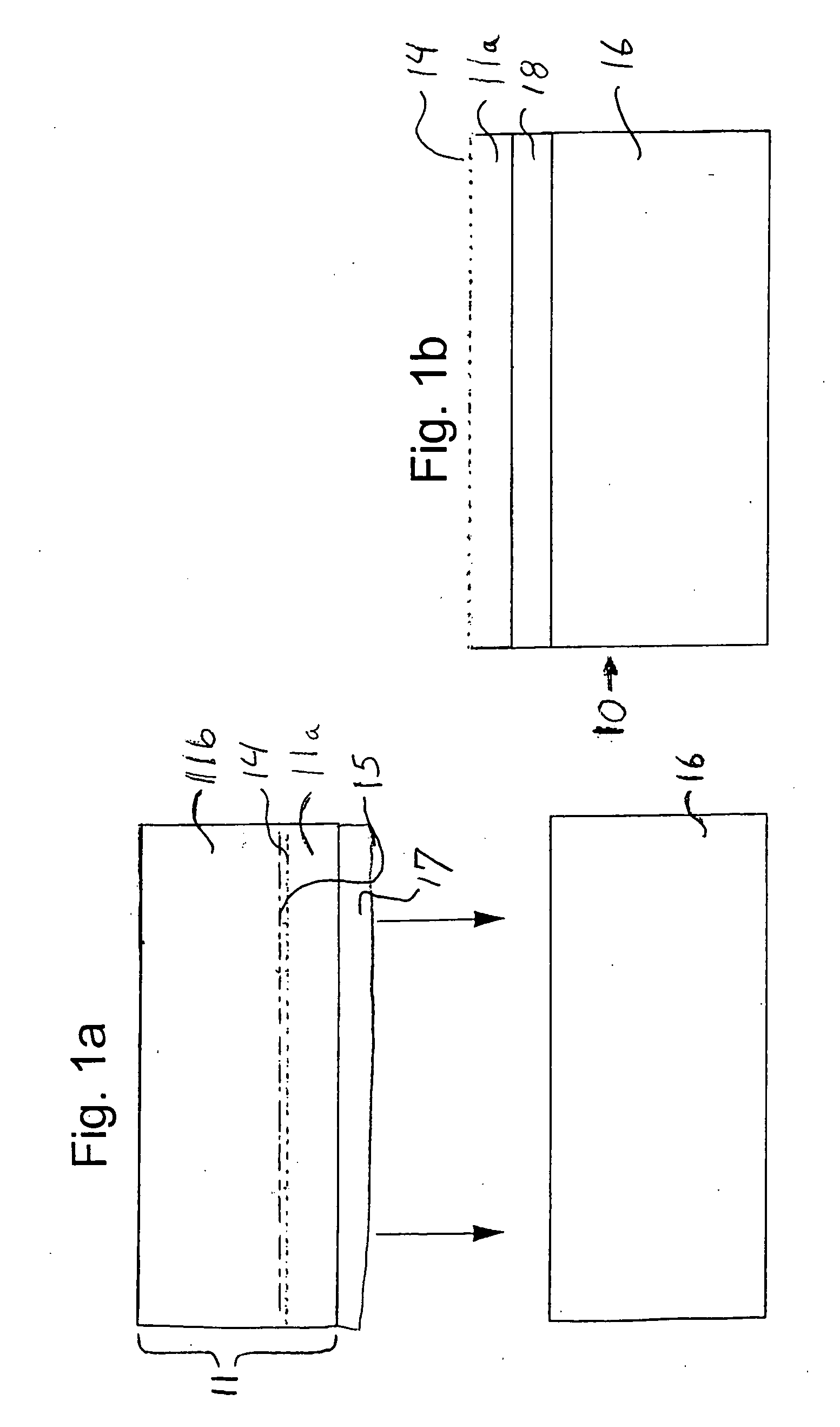
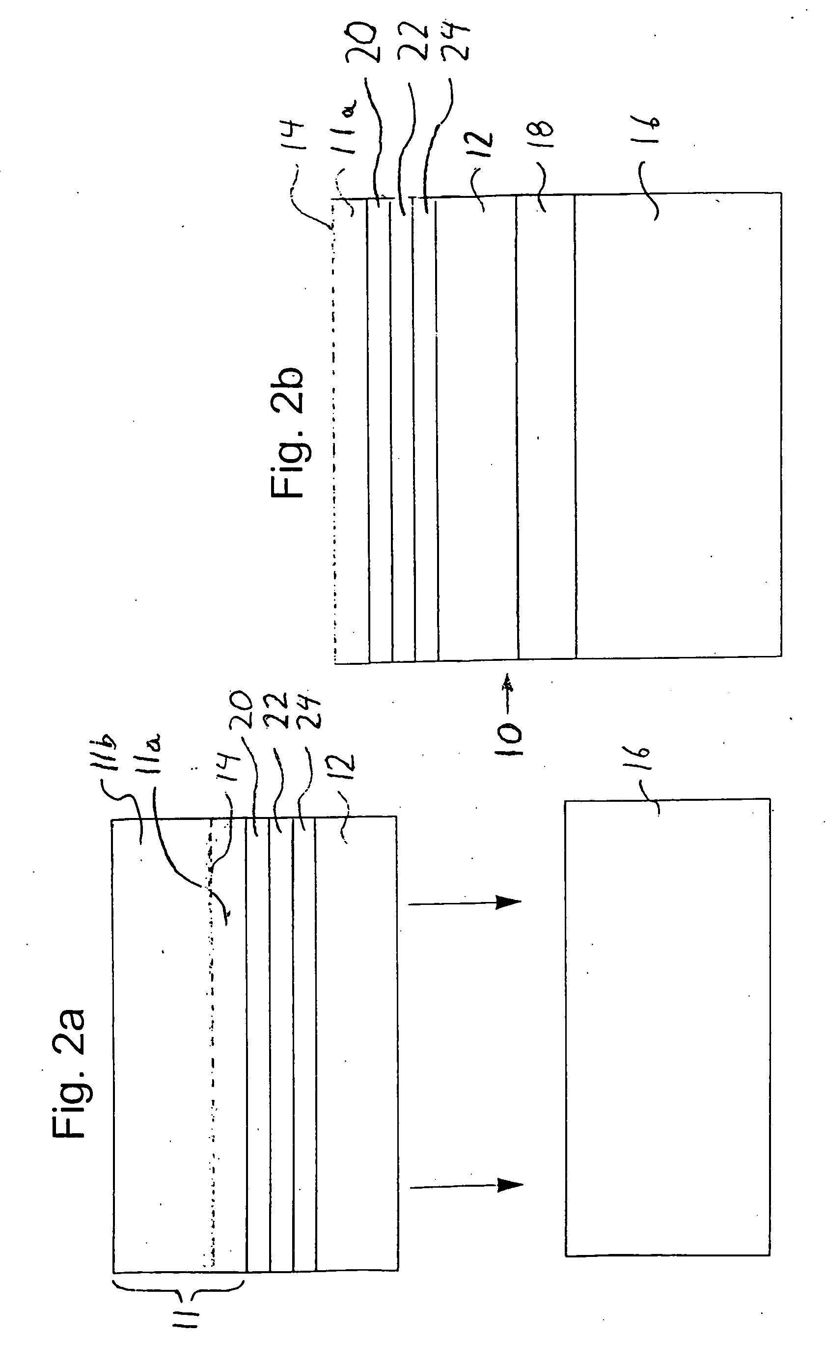
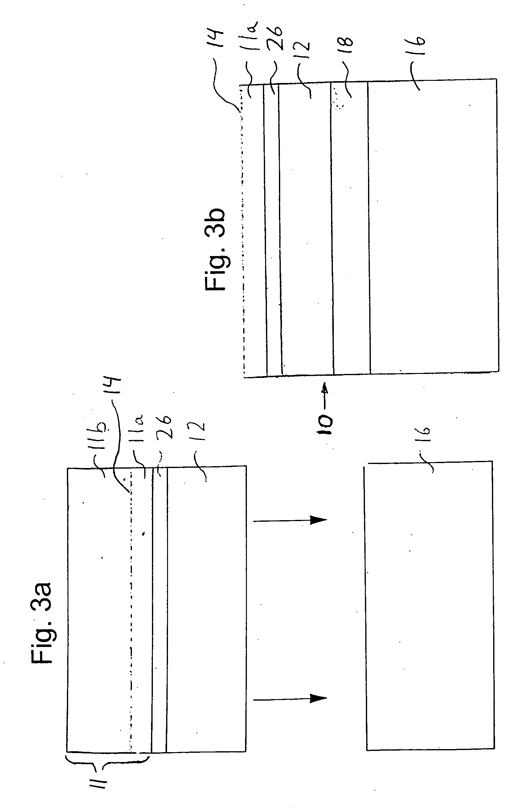
[0043] Preferred embodiments of the flexible substrate transfer method will be discussed with reference to the drawings Referring to FIG. 1a, the basic method of thin film layer transfer is illustrated. The fabrication process begins with a first substrate 11. In this embodiment, the first substrate is comprised of a single crystal semiconductor substrate. The single crystal semiconductor material is often silicon or GaAs.

[0044] A hydrogen ion implant operation is carried out next. A hydrogen ion splitting layer 14, i.e. the peak of the hydrogen implant, is implanted, within the single crystal semiconductor substrate 11. The first substrate is divided into portions 11a and 11b.

[0045] An optional stiffening material layer 17 is deposited on the surface of the single crystal substrate. The stiffening material is deposited at low temperature (below the splitting temperature for the hydrogen ion implanted layer) and can consist of deposited silicon oxide, silicon nitride, silicon, SiC, ...


PUM

PropertyMeasurementUnit
temperatureaaaaaaaaaa
splitting temperatureaaaaaaaaaa
semiconductingaaaaaaaaaa

Abstract

A method for making thin film functional material and thin film single crystal semiconductor devices having a flexible substrate is provided. In one alternative, a film layer of thin film functional material is grown on a large diameter growth substrate. One or more protective layer may be deposited on the surface of the growth substrate before the thin film functional material is deposited. Hydrogen is implanted to a selected depth within the growth substrate [or within a protective layer] to form a hydrogen ion layer. The growth substrate and associated layers are bonded to a second substrate. The layers are split along the hydrogen ion implant and the portion of the growth substrate and associated layers, which is on the side of the ion layer away from the second substrate, is removed. In another alternative, an implanted single crystal semiconductor substrate material is bonded to a flexible substrate. The substrate is split and a thin film of the single crystal semiconductor material remains bonded to the flexible substrate.

Description

[0001] 1. Field of the Invention[0002] The present invention relates to the manufacture of layered flexible semiconductor materials, and more particularly, the invention relates to a method for manufacturing a functional flexible semiconductor by transferring a single-crystal semiconductor material or thin film material to a flexible substrate.[0003] 2. Related Art[0004] There is interest within the art in cost-effective ways to improve the manufacture of devices having thin film functional materials and thin film single crystal semiconductor materials bonded on a flexible substrate; a flexible substrate being a material understood to have flexibility in excess of that of silicon. Flexible substrates offer the advantages of low weight, high flexibility and relative strength. Semiconductor devices with flexible substrates are often made by placing thin film functional materials or single layer semiconductor materials over a suitable flexible substrate.[0005] A common approach of maki...

Claims


Application Information

Patent Timeline
Patent Type & Authority Applications(United States)
IPC IPC(8): H01L21/30H01L21/46H01L21/762
CPCH01L21/76254H01L41/319H10N30/073
Inventor KUB, FRANCIS J.HOBART, KARL D.
Owner THE UNITED STATES OF AMERICA AS REPRESENTED BY THE SECRETARY OF THE NAVY
Why Eureka
Try Eureka