

Atomic reflection optical element
a technology of optical elements and atomic reflections, applied in the direction of instruments, laser details, masers, etc., can solve the problems of many problems to be solved in the direction of reflection interference devices, energy loss, and coherence disappearing
- Summary
- Abstract
- Description
- Claims
- Application Information
AI Technical Summary
Benefits of technology
Problems solved by technology
Method used
Image

Examples
first embodiment
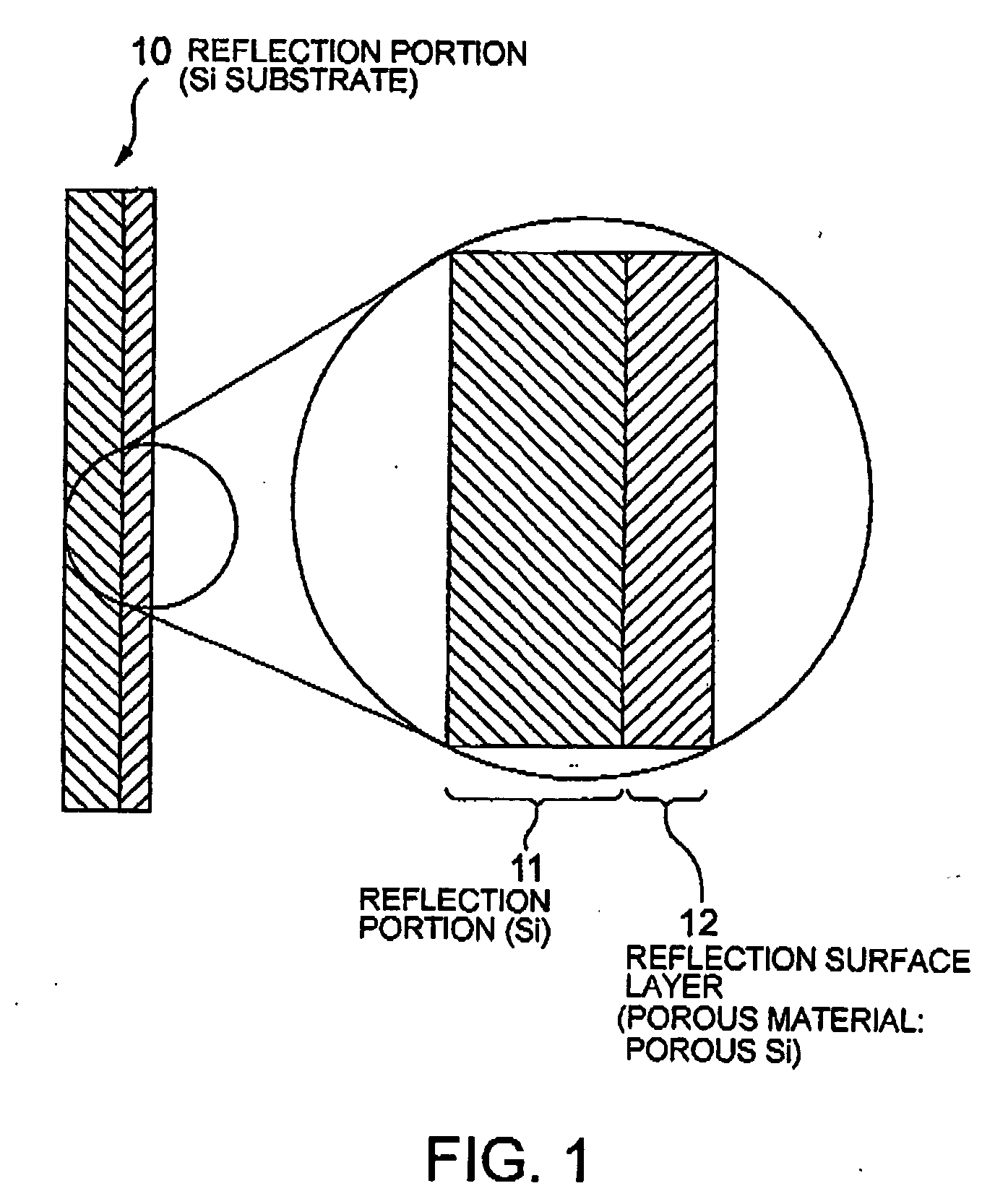
[0047] An atomic reflection optical element according to the present invention has a reflection portion 10 having a sectional structure shown in FIG. 1. The reflection portion 10 includes a reflection base layer 11, and a reflection surface layer 12 disposed on the atom incident side of the reflection base layer 11. As described above, a high reflectance can be obtained by making lower the average atomic density of a surface on which atoms are made incident, i.e., that of the reflection surface layer 12 than that in the conventional art. To achieve a low level of an average atomic density on the reflection surface, in the atomic reflection optical element according to this embodiment, the reflection surface layer 12 is made of a porous material.
[0048] Here, the surface of the porous layer does not necessarily require to be flat on the atomic level. The surface of the porous layer has only to have a flatness on the level of the wavelength of an atomic wave to be reflected, i.e., de B...
second embodiment
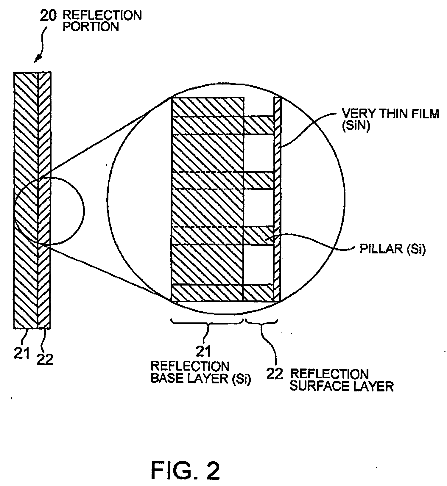
[0050] An atomic reflection optical element according to a second embodiment of the present invention is one that uses a very thin film, e.g., a silicon carbide (SiC) thin film or a silicon nitride (Si.sub.3N.sub.4) thin film, as a structure of the reflection surface. Herein, because it is difficult to hold such a very thin film in a state of a large area, pillars may be provided at appropriate positions for holding the thin film.
[0051] FIG. 2 shows an example of such an atomic reflection optical element. One portion of the substrate of the atomic reflection optical element constitutes a reflection portion 20. An enlarged view of the one portion is depicted in a circle on the right side of FIG. 2. Referring to this enlarged view, a reflection surface layer 22 is configured so that a very thin film is supported on a reflection base layer 21 by pillars. Specifically, in the example illustrated in FIG. 2, a SiN film with a thickness of 100 nm is formed on a Si substrate by CVD, and the...
third embodiment
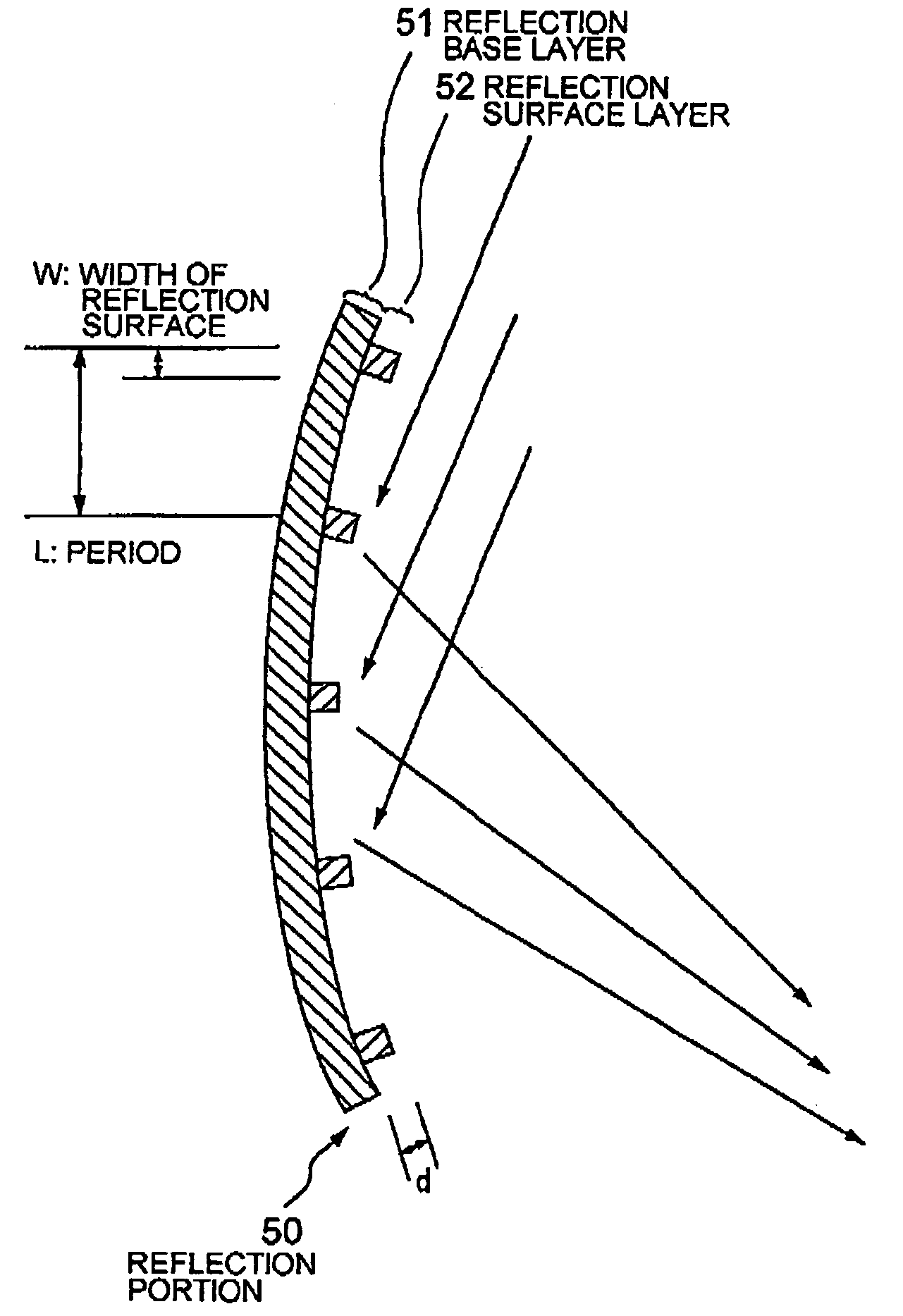
[0052] An atomic reflection optical element according to a third embodiment of the present invention is one obtained by applying the concept of the present invention to a reflection type grating.
[0053] Referring to FIG. 3, a reflection portion 30 of the atomic reflection optical element according to the third embodiment has a grating structure comprising a plurality of insular portions (reflection surfaces) and groove portions formed on the surface of a reflection base layer 31. The reflection from the grating is reflection based on total reflection up to a critical temperature, whereas over the critical temperature, reflection occurs at an angle .theta. that is given by an expression: sin .theta.=n.lambda. / L, where .lambda. denotes a de Broglie wavelength. The reflection power of the atomic wave with respect to such a grating also depends upon an atomic density on the reflection surface, which is the basic principle of the present invention. That is, the average atomic density on t...
PUM
 Abstract
Description
Claims
Application Information