

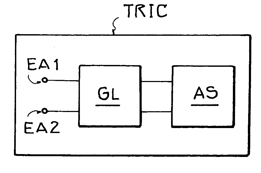
Integrated circuit for a transponder
a transponder and integrated circuit technology, applied in the direction of electric signalling details, near-field systems using receivers, instruments, etc., can solve the problems of reducing the efficiency or effectiveness of the rectifier circuit, the q-value of parasitic impedance is generally very disadvantageous, and the mismatch is difficult to reduce or eliminate, so as to and reduce the parasitic impedance
- Summary
- Abstract
- Description
- Claims
- Application Information
AI Technical Summary
Benefits of technology
Problems solved by technology
Method used
Image

Examples
first embodiment
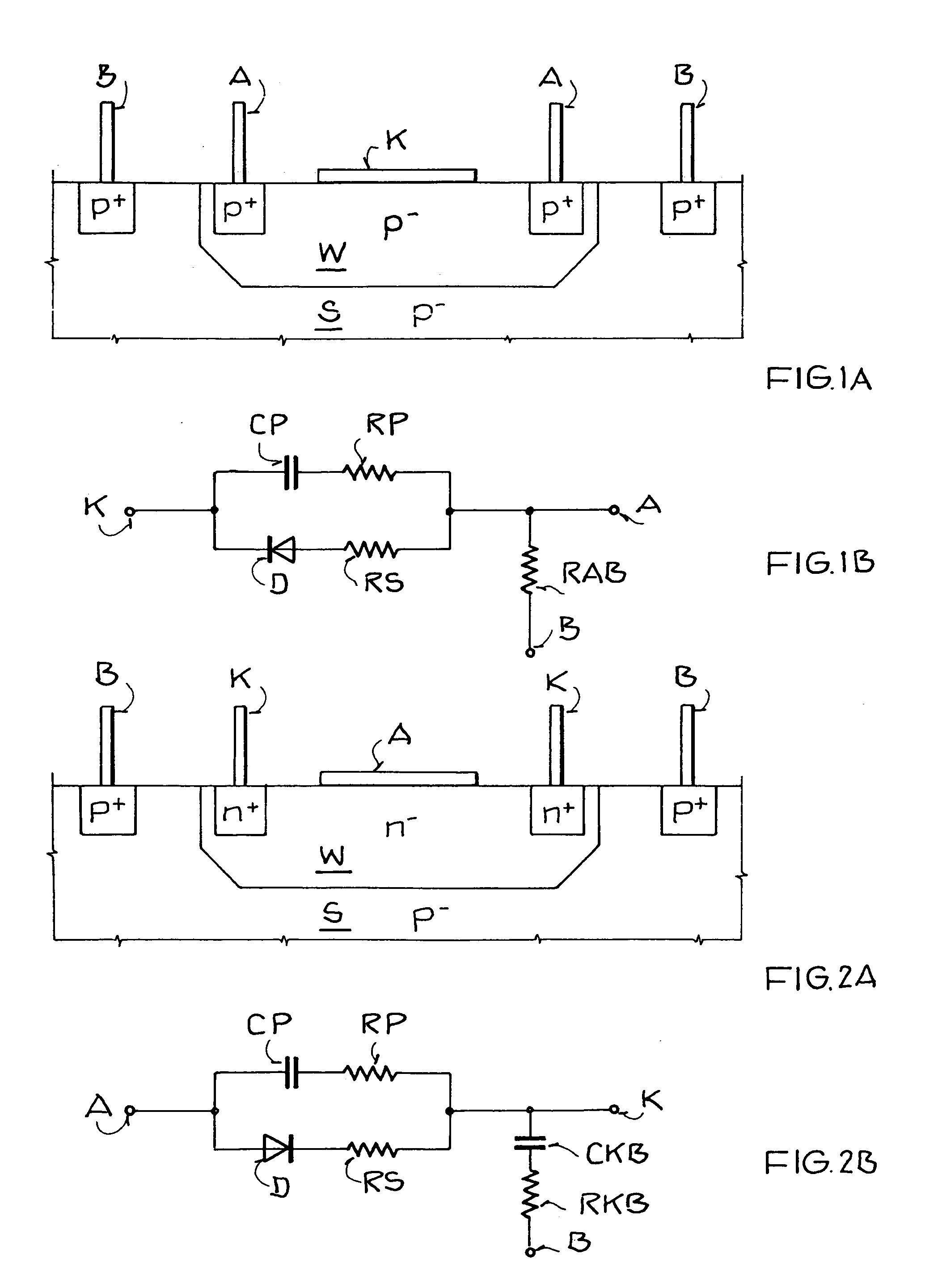
[0043] FIG. 5A shows a rectifier GL1 assembled as a Villard circuit which has been realized in this-first embodiment in a p-doped semiconductor substrate. An antenna, not shown, is connected between a ground reference potential and an input terminal EA. An operating voltage is tapped off between an output terminal AA and the ground reference potential. A capacitor C1 and a diode D2 are connected in series with each other and the series connection is connected between the input terminal EA and the output terminal AA. The diode D2 is constructed as an n-Schottky diode in accordance with the illustration of FIG. 2A. The HF-equivalent circuit of the diode D2 is shown in FIG. 2B. A cathode terminal K2 of the diode D2 is connected with the output terminal AA. A capacitor C2 connects the output terminal AA to the ground reference potential. An anode terminal A2 of the diode D2 is connected with the cathode terminal K1 of a diode D1 and with the capacitor C1. The diode D1 is constructed as ...
second embodiment
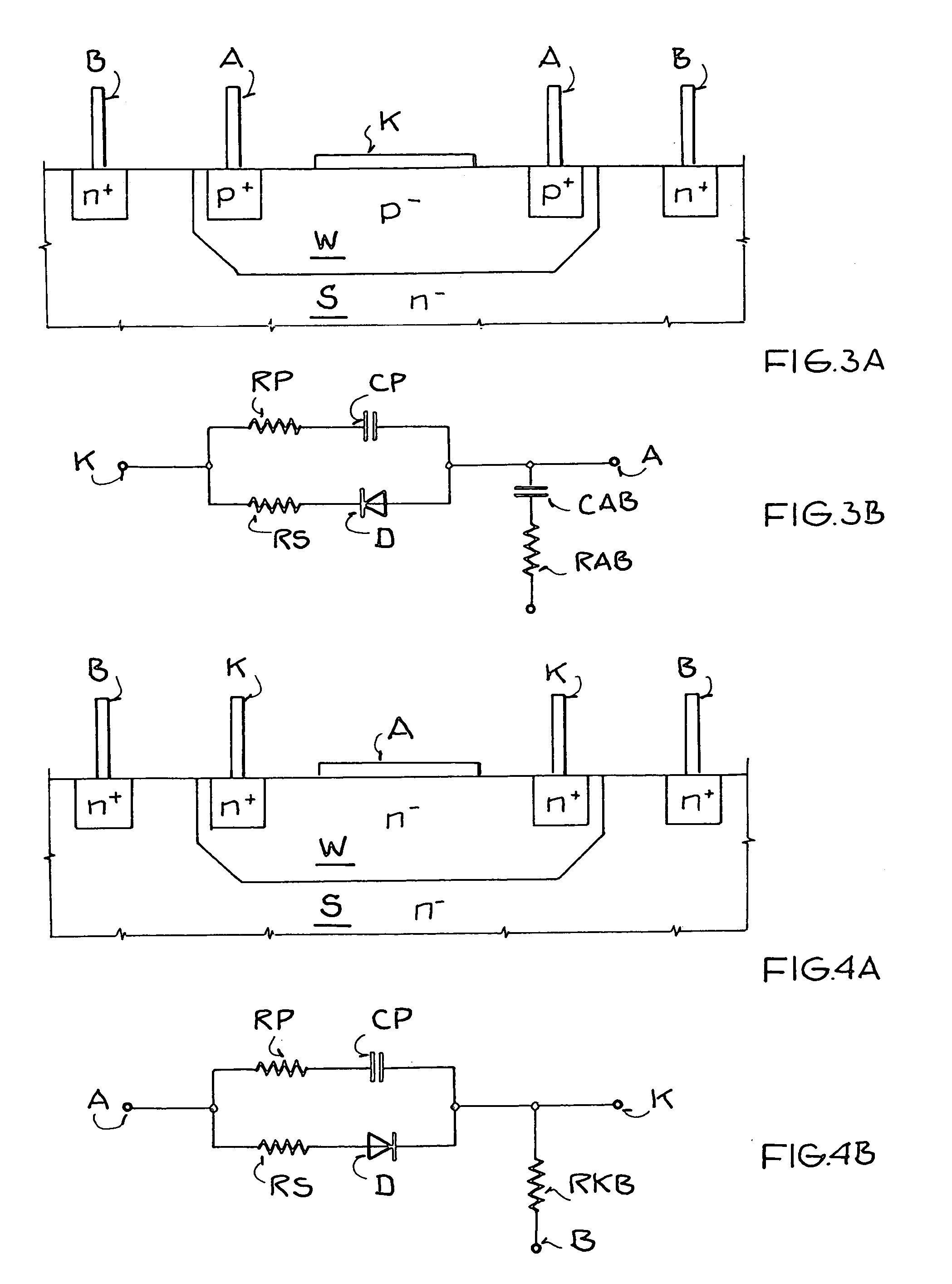
[0044] FIG. 5B shows a circuit arrangement of a rectifier GL2 in a second Villard circuit embodiment. This rectifier can also be realized in a p-doped semiconductor substrate illustrating a The difference compared to FIG. 5A is the fact that the diode D1 is constructed as an n-Schottky diode according to FIG. 2A and the diode D2 is constructed as a p-Schottky diode according to FIG. 1A. A further difference resides in that the forward direction of the diodes D1 and D2 is inverted. The anode terminal A2 of the diode D2 is connected with the output terminal AA. The cathode terminal K2 of the diode B2 is connected with the anode terminal A1 of the diode B2 and with the capacitor C1. This rectifier circuit arrangement GL2 produces a negative supply voltage at its output terminal AA. In this embodiment the parasitic impedance formed by the capacitor CKB and the resistor RKB is short-circuited because the cathode terminal K1 of the diode D1, that is its first service terminal, as well as...
PUM
 Abstract
Description
Claims
Application Information