Annealing furnace, manufacturing apparatus, annealing method and manufacturing method of electronic device

a technology of electronic devices and manufacturing equipment, applied in the direction of coatings, transistors, chemical vapor deposition coatings, etc., can solve the problems of inferior electrical characteristics, difficult to form ultra thin insulating films with a thickness of 2 nm or less, and native oxide films formed on the surface of si substrates, etc., to achieve the effect of reducing the thickness of the film, and improving the electrical performan

Inactive Publication Date: 2004-12-30
KK TOSHIBA
View PDF12 Cites 57 Cited by
  • Summary
  • Abstract
  • Description
  • Claims
  • Application Information

AI Technical Summary

Problems solved by technology

Thus, it is difficult to form ultra thin insulating films with a thickness of 2 nm or less with great repeatability at a high oxidation temperature of, for example, approximately 1000.degree. C.
The native oxide film, which is formed on the surface of the Si substrate, has inferior electrical characteristics.
Thus, the thermal oxide film having good electrical characteristics can be formed in the RTO, but it is extremely difficult to control the thickness of the film to be 2 nm or less since the native oxide film is formed before the thermal oxidation process.

Method used


Image

  • Annealing furnace, manufacturing apparatus, annealing method and manufacturing method of electronic device
  • Annealing furnace, manufacturing apparatus, annealing method and manufacturing method of electronic device
  • Annealing furnace, manufacturing apparatus, annealing method and manufacturing method of electronic device

Examples


first embodiment

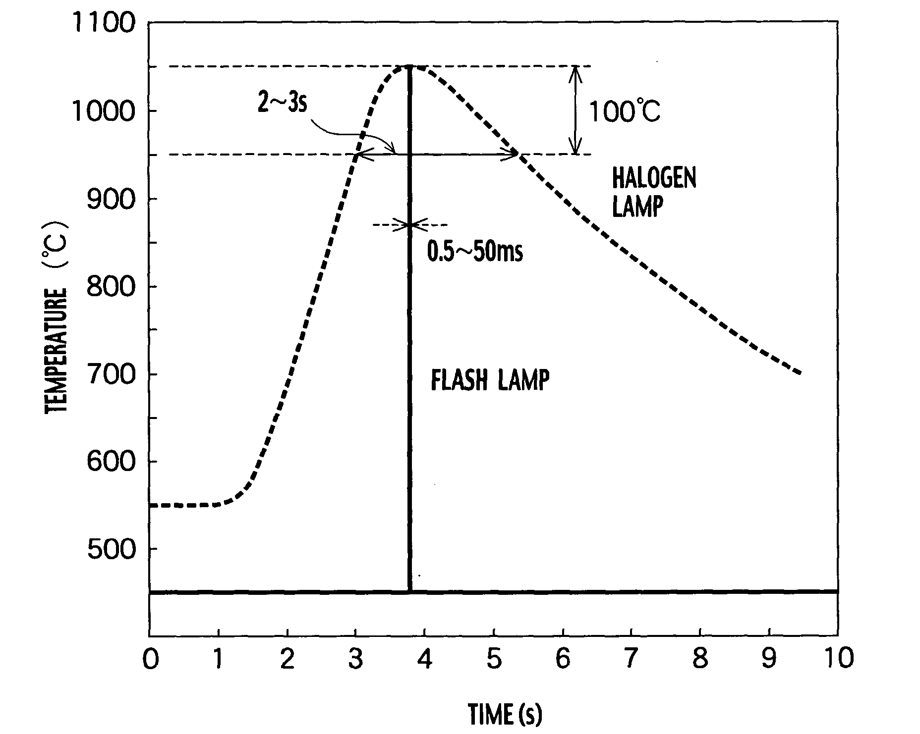
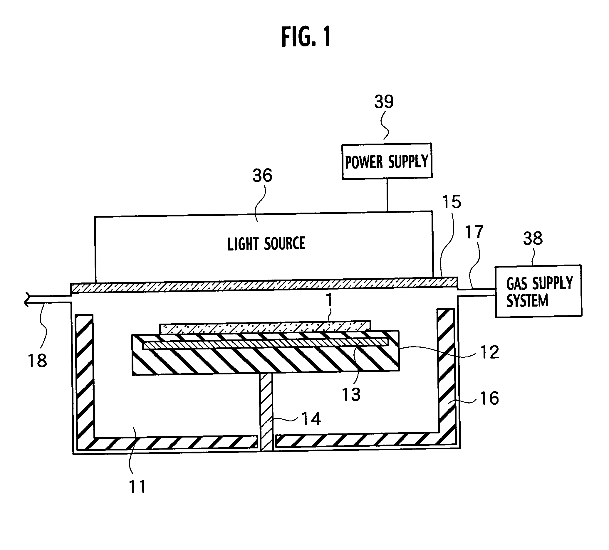
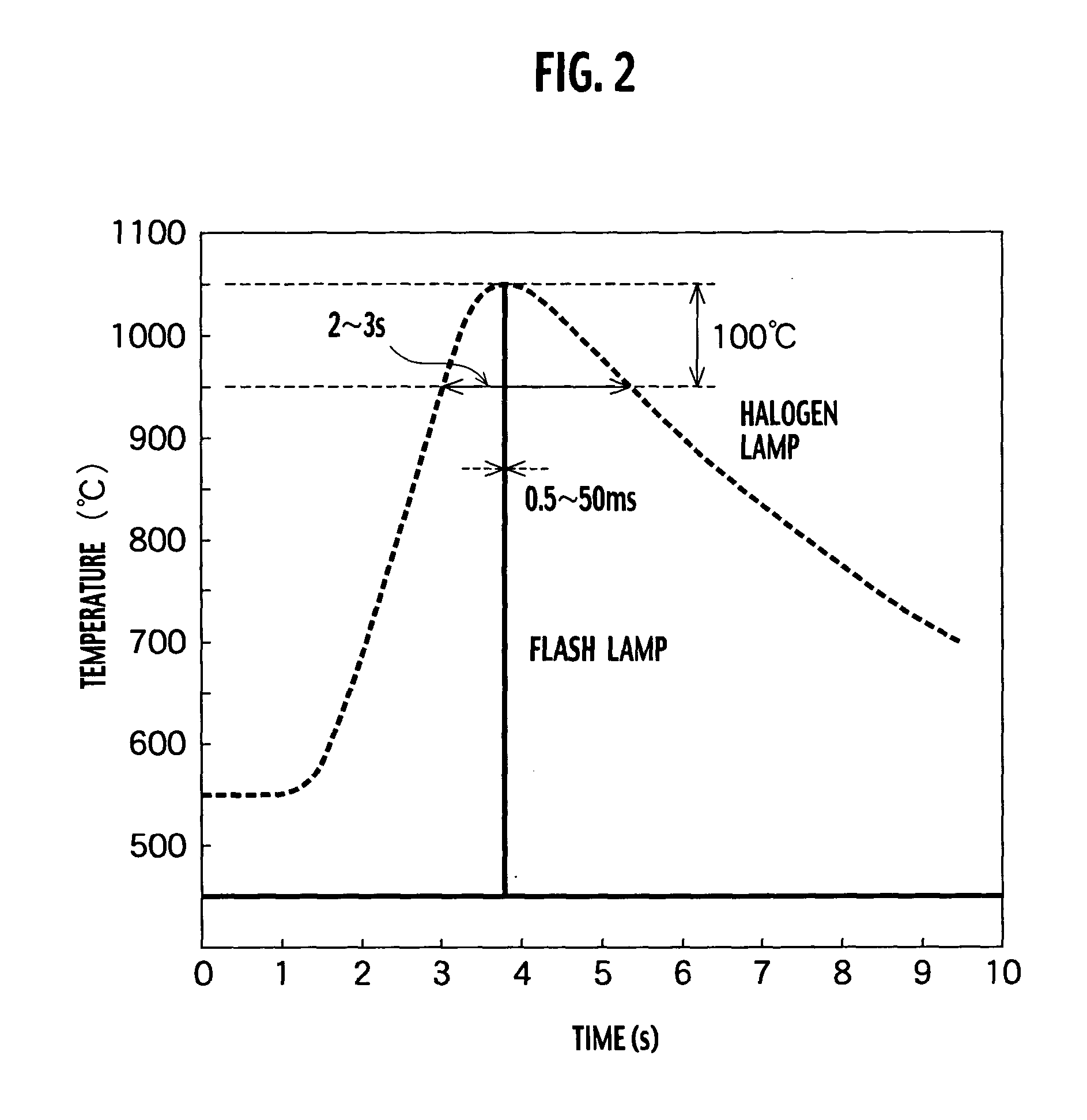
[0034] As shown in FIG. 1, an annealing furnace according to the present invention includes a processing chamber 11, a susceptor 12, an introduction conduit 17, an exhaust conduit 18, a transparent window 15 and a main heater 36. Herein, a substrate 1 such as a semiconductor substrate is processed in the processing chamber 11. The susceptor 12, on which the substrate 1 is loaded, is located in the processing chamber 11. The introduction conduit 17 supplies gas to the surface of the substrate 1. The exhaust conduit 18 exhausts gas from the processing chamber 11. The transparent window 15 is located facing the susceptor 12 on the top of the processing chamber 11. The main heater 36 irradiates the surface of the substrate 1 from the transparent window 15 with pulsed light.

[0035] The processing chamber 11 is made of a metal such as stainless steel. The susceptor 12, on which the substrate 1 is loaded, is located on the top of a support shaft 14 installed perpendicular to the bottom of t...

second embodiment

[0044] As shown in FIG. 6, in a manufacturing apparatus according to a second embodiment of the present invention, first and second processing apparatuses 21 and 22 are connected to a transfer chamber 30 through gate valves 34a and 34b, respectively. The first processing apparatus 21 has a first processing chamber 11a in which a first susceptor 12a is located, and a substrate 1 is loaded on the first susceptor 12a. The second processing apparatus 22 has a second processing chamber 11b in which a second susceptor 12b is located, and a substrate 1a is loaded on the second susceptor 12b. To the first and second processing chambers 11a and 11b, first and second introduction conduits 17a and 17b are connected to supply a variety of gases from a gas supply system 38. To the transfer chamber 30, first and second cassette chambers 10 and 20 are installed. In the first cassette chamber 10, a wafer cassette storing the substrates 1 and 1a is placed. In the second cassette chamber 20, a wafer ...

third embodiment

[0071] As shown in FIG. 19, a manufacturing apparatus according to a third embodiment of the present invention includes first and second processing apparatuses 21a and 22a. In the second embodiment, the first and second processing apparatuses 21 and 22 are both used to form the insulting film. The third embodiment differs from the second embodiment in that a pretreatment of removing a native oxide film on the surface of a substrate 1 is performed in the first processing apparatus 21a, and a processing of forming an insulating film is performed in the second processing apparatus 22a. Other than that, the third embodiment is the same as the second embodiment. Thus, redundant descriptions will be omitted.

[0072] In the first processing apparatus 21a, pretreatment gas for removing a native oxide film on the surface of a substrate 1 loaded on a first susceptor 12a is supplied from a gas supply system 38. For pretreatment gas, reduction gas such as H.sub.2 gas, mixed gas containing H.sub.2...


PUM

PropertyMeasurementUnit
temperatureaaaaaaaaaa
thicknessaaaaaaaaaa
thickaaaaaaaaaa

Abstract

An annealing furnace, includes a processing chamber configured to store a substrate; a susceptor located in the processing chamber so as to load the substrate and having an auxiliary heater for heating the substrate at 650° C. or less, the susceptor having a surface being made of quartz; a gas supply system configured to supply a gas required for a thermal processing on the substrate in parallel to a surface of the substrate; a transparent window located on an upper part of the processing chamber facing the susceptor; and a main heater configured to irradiate a pulsed light on the surface of the substrate to heat the substrate from the transparent window, the pulsed light having a pulse duration of approximately 0.1 ms to 200 ms and having a plurality of emission wavelengths.

Description

[0001] This application is based upon and claims the benefit of priority from prior Japanese Patent Application P2003-181731 filed on Jun. 25, 2003; the entire contents of which are incorporated by reference herein.[0002] 1. Field of the Invention[0003] The present invention relates to an annealing furnace for processing the surface of an electronic device in the manufacturing process of the electronic device and, in particular, to a manufacturing apparatus and an annealing method of forming a thin insulating film by use of a heating lamp and to a manufacturing method of an electronic device.[0004] 2. Description of the Related Art[0005] Large scale integrated (LSI) circuits have been becoming larger to improve their performance, and at the same time, finer elements have been advancing more rapidly than ever. When a metal-insulator-semiconductor field effect transistor (MISFET) is used, the electrical thickness of a gate insulating film is required to become thinner in correspondenc...

Claims


Application Information

Patent Timeline
Patent Type & Authority Applications(United States)
IPC IPC(8): H01L21/00H01L21/02H01L21/28H01L21/31H01L21/306H01L21/314H01L21/316H01L21/318H01L21/32H01L21/8234H01L27/088H01L29/51H01L29/78
CPCH01L21/02046H01L21/28185H01L21/28202H01L21/28211H01L21/28238H01L21/3144H01L21/32H01L21/67115H01L21/67155H01L21/823462H01L29/513H01L29/518H01L21/02233H01L21/02247H01L21/31H01L21/02
Inventor SUGURO, KYOICHIITO, TAKAYUKIITANI, TAKAHARU
Owner KK TOSHIBA
Why Eureka
Try Eureka