Light emitting device and method for manufacturing the same

a technology of light emitting devices and light emitting elements, which is applied in the manufacture of electrode systems, electric discharge tubes/lamps, and discharge tubes luminescnet screens, etc., can solve the problems partial decrease in luminance, and generation of non-light emitting regions, so as to reduce or eliminate generation

Inactive Publication Date: 2005-01-06
SEMICON ENERGY LAB CO LTD
View PDF3 Cites 37 Cited by
  • Summary
  • Abstract
  • Description
  • Claims
  • Application Information

AI Technical Summary

Benefits of technology

It is an objective of the present invention to reduce or eliminate generation of the above described various defective modes of the light emitting element containing an organic compound.
Inventors of the present invention assume that random arrangement of organic compound molecules in a layer containing an organic compound causes the light emitting element containing an organic compound to be easily deteriorated. According to the present invention, molecules in the layer containing an organic compound are arranged (or oriented) in a certain direction. Specifically, it is preferable to arrange molecules with a structure having a high planarity.
The organic compound molecules may be arranged by electrolytic polymerization after performing surface modification for arranging the molecules. The molecules are easily arranged in a direction of current by forming a layer containing an organic compound with current applied in one direction after performing surface modification on an electrode or forming an ultra thin film by application in advance. The molecules may be arranged by intermolecular electrostatic interaction.
A light emitting element (EL element) including an EL layer has a structure in which the EL layer is interposed between a pair of electrodes. Typically, an EL layer has a laminate structure: a hole transporting layer; a light emitting layer; an electron transport layer. The structure provides extremely high light emission efficiency, and is adopted in most of light emitting devices that are currently under development.

Problems solved by technology

A light emitting element containing an organic compound has a defect to be easily deteriorated by various factors; therefore, it is the biggest issue to obtain high reliability (longer lifetime) of the light emitting element.
The light emitting element containing an organic compound is easily deteriorated, and a defective condition in which a partial decrease in luminance occurs or a non-light-emitting region is generated is observed.

Method used


Image

  • Light emitting device and method for manufacturing the same
  • Light emitting device and method for manufacturing the same
  • Light emitting device and method for manufacturing the same

Examples


embodiment mode 1

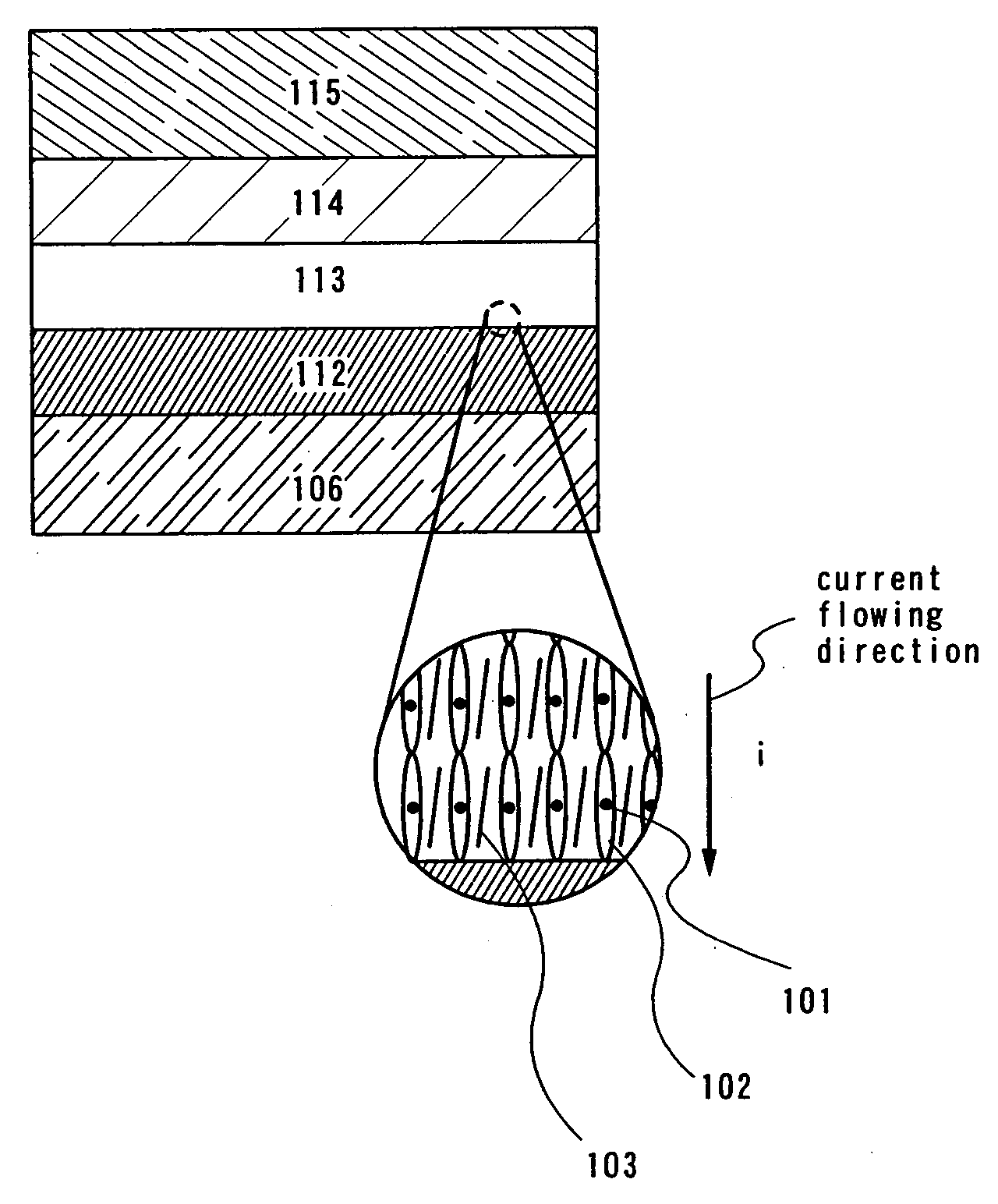
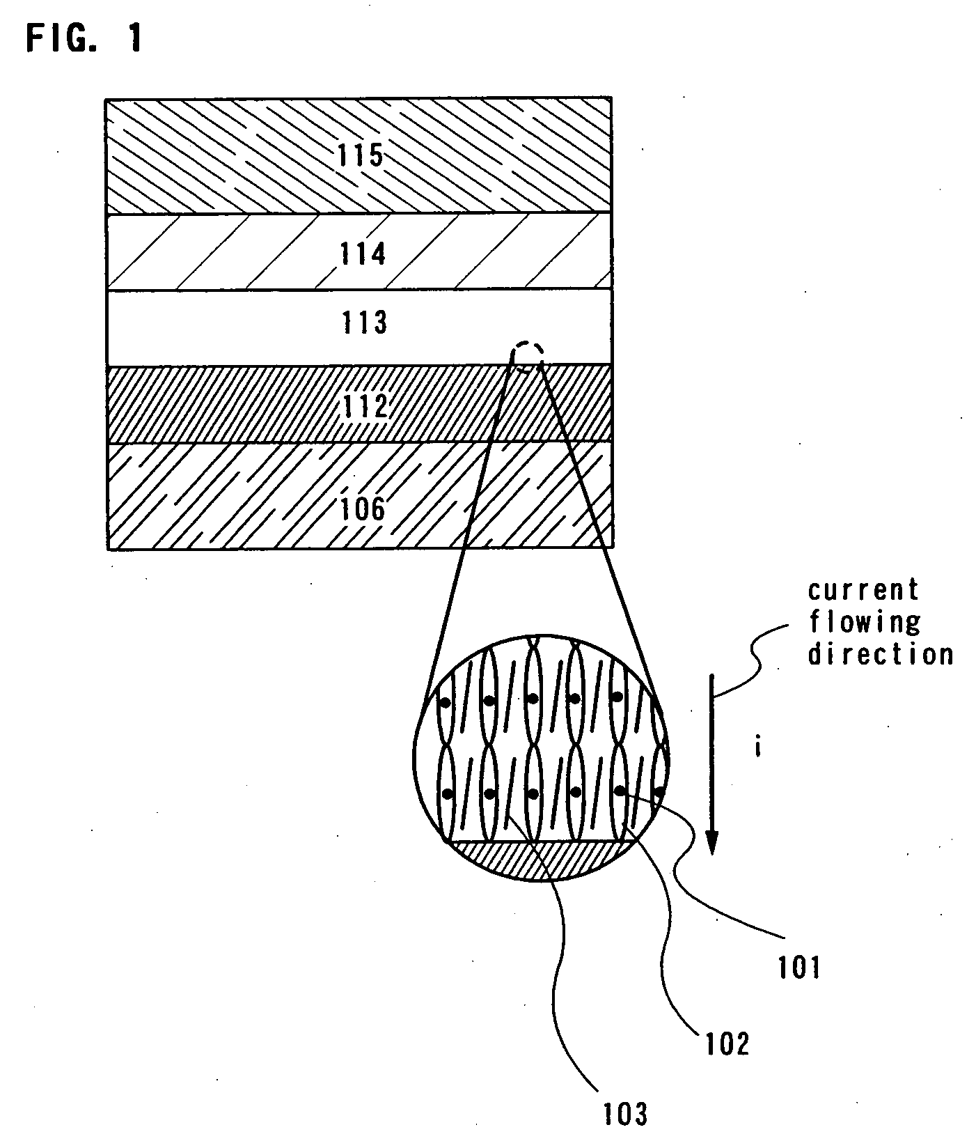
FIG. 1 shows a schematic diagram of the present invention.

According to the invention, an electroluminescent layer is formed over an electrode (first electrode) 106 that is formed over a substrate (not shown) as shown in FIG. 1. As a material for the substrate, glass, quartz, transparent plastics, or the like can be used.

In addition, the first electrode 106 may function as either an anode or a cathode. A plurality of the first electrodes 106 may be pattern formed over the substrate. In the case of an active matrix light emitting device, a plurality of TFTs are formed over the substrate. The first electrodes 106 are electrically connected to source electrodes or drain electrodes of the TFTs and are arranged in a matrix configuration.

In addition, in the case where the first electrode 106 functions as an anode, metals, alloys, electrically conductive compounds, and mixtures of these materials, which have large work functions (at least 4.0 eV), can preferably be used as anode mater...

embodiment mode 2

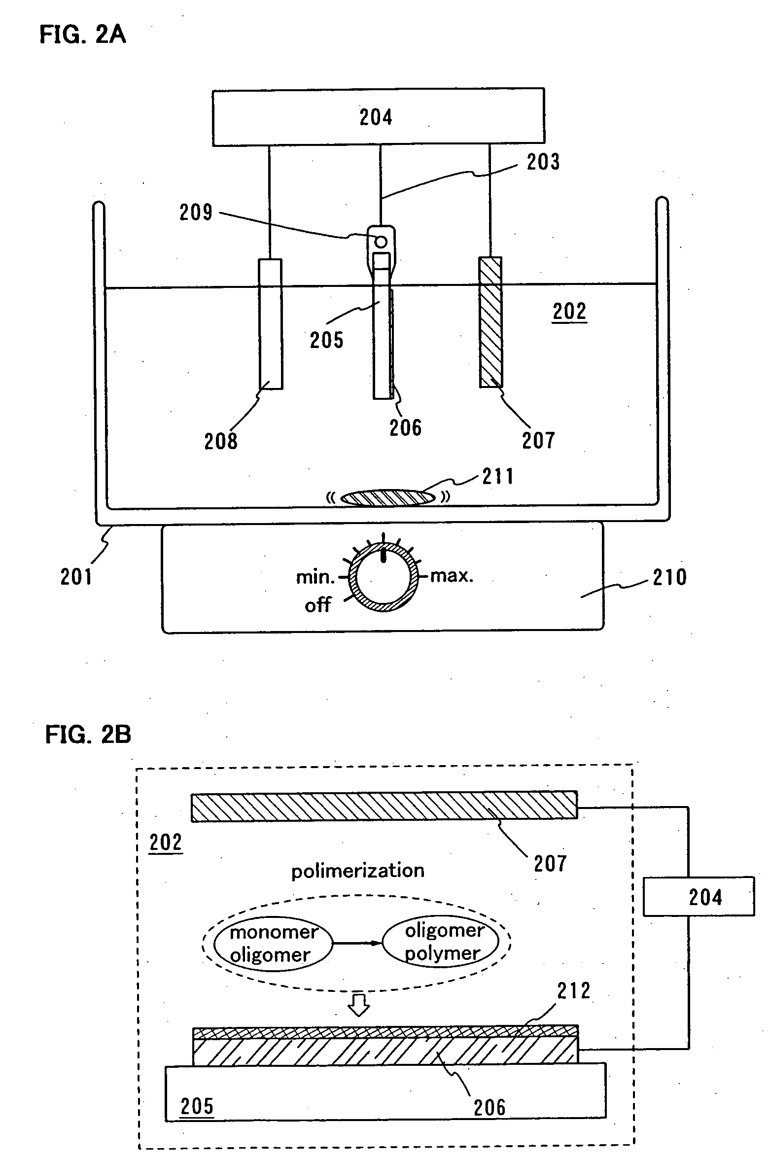
An example of forming a layer containing an organic compound by electrolytic polymerization is described as an example of a method for orienting organic compound molecules. After performing surface modification on an electrode or forming an ultra thin film (not shown) in advance by application, a layer containing an organic compound is formed by electrolytic polymerization.

As shown in FIG. 2A, a reaction tank 201 holds an electrolytic solution 202, and a substrate 205 on which a first electrode 206 electrically connected to a power source 204 via a wiring 203 is formed, a counter electrode 207, and a reference electrode 208 are immersed in the electrolytic solution 202. In addition, the substrate 205 is secured by a support medium 209 that electrically connects the first electrode (anode or cathode, here, an anode) 206 to the wiring 203.

The power source 204 includes a potentiostat which is capable of applying a constant electric potential and a coulombmeter which measures an am...

embodiment mode 3

Another example of a method for orienting organic compound molecules is described here.

FIG. 3 shows a light emitting element in which layers containing an organic compound is used as electroluminescent layers 312 to 314, a first electrode 306 is used as a cathode, and a second electrode 315 is used as an anode. An organic compound molecule 302 shown in Structural Formula 5 is reacted with a surface of the first electrode containing Au, Pt, or Ag to form an Au—S bond, a Pt—S bond, or an Ag—S bond.

[Structural Formula 5]

HS—(CH2)n—X—Ar   (5)

Note that n=2 to 6, or 8. Structural Formula 6 shows an example of X in Structural Formula 5, and Structural Formula 7 shows an example of Ar. Ar here is a general abbreviation for an aryl (aromatic) group.

[Structural Formula 6]

X=nil, —CnH2n—, —O—, —S—, —N(R)—, —Si(R2)— (R═H, CnH2n, Ar)   (6)

[Structural Formula 7]

Combination of X and Ar may be arbitrary. In addition, Structural Formula 5 may not include X.

Solution including these materia...


PUM

PropertyMeasurementUnit
work functionsaaaaaaaaaa
thicknessaaaaaaaaaa

Abstract

A light emitting element containing an organic compound has a defect that the light emitting element is easily deteriorated by various factors; therefore, it is the biggest issue of the light emitting element that the light emitting element is formed with high reliability (longer lifetime). An objective of the present invention is to reduce or eliminate generation of the above described various defective modes of the light emitting element containing an organic compound. According to the present invention, current efficiency-luminance characteristics can be improved by orienting organic compound molecules in an applying direction of current. In addition, deterioration can be prevented by using a crystallization inhibitor.

Description

BACKGROUND OF THE INVENTION 1. Field of the Invention The present invention relates to an organic light emitting element including an anode, a cathode, and a layer containing an organic compound (hereinafter, referred to as an electroluminescent layer) that generates light by applying an electric field through itself; and a light emitting device including the light emitting element. Specifically, the present invention relates to an organic light emitting element that exhibits white light emission and a full color light emitting device including the white light emitting element. As used herein, the term “light emitting device” refers to an image display device or a light source (including a lighting system). Further, a module having a light emitting element attached with a connector such as an FPC (Flexible Printed Circuit), a TAB (Tape Automated Bonding), or a TCP (Tape Carrier Package); a module having a TAB or a TCP provided with a printed wiring board at the tip thereof; and a...

Claims


Application Information

Patent Timeline
Patent Type & Authority Applications(United States)
IPC IPC(8): H01L51/50H01L51/00H01L51/52H01L51/56H05B33/10H05B33/12H05B33/14H05B33/22H05B33/26
CPCH01L51/0012H01L51/5012H01L51/5203Y10S428/917H05B33/10H05B33/14H01L51/5237H10K71/191H10K50/11H10K50/846H10K50/8426H10K50/844H10K59/805H10K50/805
Inventor NOMURA, RYOJIABE, HIROKOYAMAZAKI, SHUNPEI
Owner SEMICON ENERGY LAB CO LTD
Why Eureka
Try Eureka