Method for fabricating a laminate film, laminate film, and method for fabricating a display device

a technology of laminate film and display device, which is applied in the direction of identification means, instruments, polarising elements, etc., can solve the problems of large dependence on viewing angle, reduced display quality, and viewer's failure to correctly recognize display images, so as to reduce the generation of defects, prevent deformation, and easy bonding and fixing

Inactive Publication Date: 2005-01-06
SHARP KK
View PDF26 Cites 24 Cited by
  • Summary
  • Abstract
  • Description
  • Claims
  • Application Information

AI Technical Summary

Benefits of technology

[0047] In particular, when the adhesive layer for bonding the optical film and the transparent support together is made of a photocurable resin, the optical film and the transparent support can be easily bonded and fixed together. This reduces generation of defects due to scars and external force.
[0048] By placing a surface protection film on the outer surface of the adhesive layer of the adhesive film and setting the thickness t of the surface protection film in the range of 0.035 mm≦t≦0.2 mm, the adhesive layer is prevented from deforming due to existence of foreign matters and external force before curing. As a result, bonding between the light diverging element and the transparent member is facilitated.
[0049] The method for fabricating a display device according to the present invention also has the function described above in relation with the method for fabricating a laminate film. In particular, in the case of using a liquid crystal display element as the display element, waves tend to be generated on the surface of a polarizing plate or a phase plate of the display element. When an optical film is bonded to the polarizing plate or the phase plate in an attempt to improve the characteristics of the display element, the waves of the polarizing plate or the phase plate are transferred to the optical film. According to the fabrication method of the present invention, however, the laminate film is bonded to the display element after the adhesive layer is cured to a degree that the adhesion state between the optical film and the adhesive layer no more changes. Therefore, it is possible to prevent the uneven surface of the display element from influencing the optical film, and thus prevent deterioration in display quality. In particular, when a lens sheet as the optical film is bonded to a liquid crystal display element by the fabrication method according to the present invention, the resultant liquid crystal display device can exhibit high display quality with an improved viewing angle characteristic.
[0050] By placing a surface protection film on the outer surface of the adhesive layer formed on the transparent support and setting the thickness t of the surface protection film in the range of 0.035 mm≦t≦0.2 mm, the adhesive layer is prevented from deforming due to existence of foreign matters and external force before curing. As a result, bonding between the optical film and the transparent support is facilitated. In particular, spot defects and bar-shaped defects influence the optical performance of the light diverging element. A defect having a diameter of 0.1 mm or more will be observed as a panel defect, causing significant deterioration in display quality.
[0051] By controlling the thickness of the surface protection film, the number of spot defects and bar-shaped defects can be markedly reduced. For example, while the number of defects is 200 pieces / m2 when the thickness of the surface protection film is 0.02 mm, it can be as small as 50 pices / m2 when the thickness is 0.035 mm. For a 20-inch liquid crystal display device, for example, about 25 defects can be reduced to 10 pieces or less. The display quality therefore improves.
[0052] Although a thicker surface protection film can reduce the number of defects, it increases the cost since the material cost is higher. Therefore, the thickness is preferably 0.2 mm or less.

Problems solved by technology

A major problem relating to such liquid crystal display devices is that the viewing angle dependence is large.
When the screen of a display device is viewed from a direction tilting by an angle exceeding a certain angle range, an image that should correctly be displayed in black appears whitish, or reversal in gray scale levels is observed, causing reduction in display quality.
From theses viewing directions, the viewer fails to correctly recognize the display image.
By the above construction, however, the viewing angle range is still insufficient.
The above conventional techniques have the following problems.
As a result, the display quality greatly deteriorates.
No means for solving the above problems have been mentioned in the prior art literature.

Method used


Image

  • Method for fabricating a laminate film, laminate film, and method for fabricating a display device
  • Method for fabricating a laminate film, laminate film, and method for fabricating a display device
  • Method for fabricating a laminate film, laminate film, and method for fabricating a display device

Examples


embodiment 1

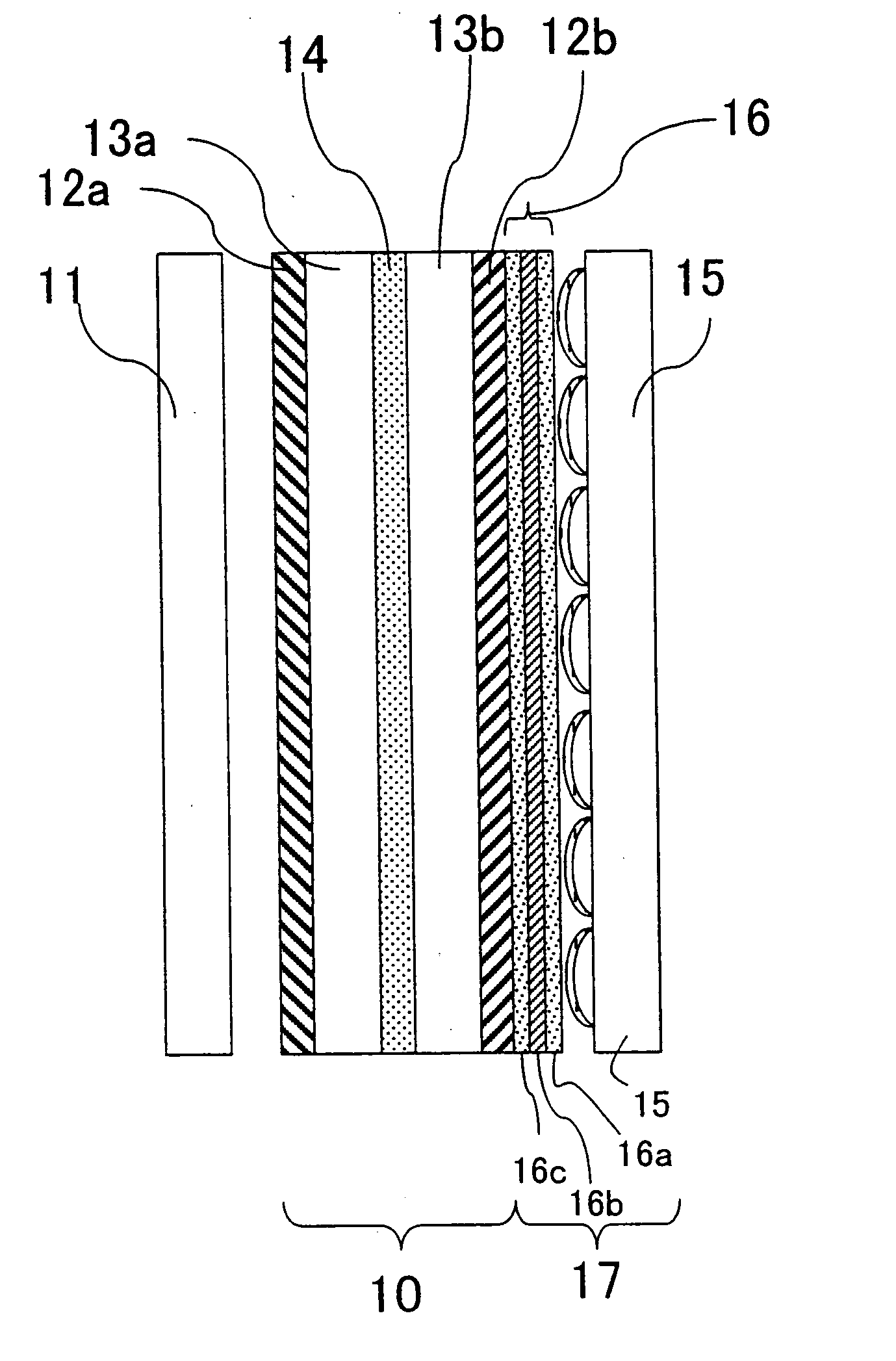
[0078]FIG. 1 is a cross-sectional view of a liquid crystal display device used in Embodiment 1 of the present invention. Referring to FIG. 1, the liquid crystal display device in this embodiment includes a surface illuminant 11, a liquid crystal display element 10 and a laminate film 17 which includes an adhesive film 16, and a lens sheet (lens film) 15 as an optical film.

[0079] The liquid crystal display element 10 is essentially including: an active matrix substrate 13a including thin film transistors (TFTs), transparent pixel electrodes, and the like formed in a matrix on a transparent substrate made of glass or plastic; a counter substrate 13b including transparent electrodes and color filters formed on a transparent substrate made of glass or plastic; liquid crystal material 14 as a display medium sealed in a space between the two substrates; and a pair of polarizing plates (polarizing films) 12a and 12b placed to sandwich the two substrates.

[0080] In this embodiment, twisted...

embodiment 2

[0125] Embodiment 2 of the present invention will be described with reference to FIGS. 14 to 21.

[0126]FIG. 14 is a cross-sectional view illustrating a liquid crystal display device used in Embodiment 2 of the present invention. Referring to FIG. 14, the illustrated liquid crystal display device, which is of a reflection type, includes a reflection type liquid crystal display element 140 and a laminate film 147. The laminate film 147 includes a transparent member 145 and a prism sheet 146 as an optical film, and the transparent member 145 includes a first adhesive layer 145a, a transparent support 145b, and a second adhesive layer 145c.

[0127] The reflection type liquid crystal display element 140 is essentially including: an active matrix substrate 141a including thin film transistors (TFTs) and transparent pixel electrodes arranged in a matrix and a reflector 142 formed on a substrate made of glass, plastic, a monocrystalline silicon, or the like; TN liquid crystal material 143 ha...


PUM

PropertyMeasurementUnit
thicknessaaaaaaaaaa
diameteraaaaaaaaaa
thicknessaaaaaaaaaa

Abstract

Adhesive layers are formed on the two opposing surfaces of a transparent support. At least one of the adhesive layers is made of a material of which the cured state may be changed. The adhesive layer is irradiated with light and a lens sheet is then pressed against the adhesive layer. The adhesive layer is cured. In this illustrative way, a laminate film of the lens sheet fixed to the transparent support via the adhesive layer may be obtained. The laminate film may be bonded to a polarizing plate on the viewer's side of a liquid crystal display element via the other adhesive layer.

Description

BACKGROUND OF THE INVENTION [0001] 1. Field of the Invention [0002] The present invention relates to a method for fabricating a laminate film, and in particular, relates to a method for fabricating a display device (e.g. liquid crystal display device) using a laminate film and having improved viewing angle characteristic. [0003] 2. Description of Related Art [0004] Liquid crystal display devices, which typify flat panel displays, have features of being lightweight, thin, and low in power consumption, compared with CRTs, and thus find applications in wide-range fields such as OA apparatus, car-mounted TV sets, car navigation systems, and monitors for video cameras. [0005] A major problem relating to such liquid crystal display devices is that the viewing angle dependence is large. The viewing angle dependence refers to the following phenomenon, for example. When the screen of a display device is viewed from a direction tilting by an angle exceeding a certain angle range, an image tha...

Claims


Application Information

Patent Timeline
Patent Type & Authority Applications(United States)
IPC IPC(8): G02B5/02B29C39/10B29C65/48B29L9/00B29L11/00B32B7/02G02B3/00G02B5/30G02F1/1335G02F1/13363G09F9/00
CPCG02F1/1335G02F1/133504G02F1/133526Y10T428/10Y10T428/1059Y10T428/24355Y10T428/1481C09K2323/00C09K2323/05
Inventor SUMIDA, YUKIHIROSATO, TAKASHIKIHARA, HIDENORIWATANABE, NORIKO
Owner SHARP KK
Why Eureka
Try Eureka